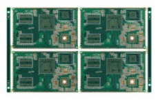
Structure level of flexible circuit board
Since the continuous development of PCB circuit boards, many types have been derived, but most of them can be divided into two types: rigid and flexible circuit boards, and now we will talk about the structure of flexible circuit boards.
Generally, PCB circuit boards are classified according to the number and thickness of conductive copper foil. These can be divided into single-layer boards, double-layer boards, multilayer boards and double-sided boards. The structures of these are also different. Next, Let's introduce in detail where these different features are.
Single-layer board structure: This is a relatively simple flexible board. Generally, it is a set of raw materials purchased with base material + transparent glue + copper foil, and protective film + transparent glue is another purchased raw material;, The copper foil needs to carry out etching and other treatment processes to obtain the necessary circuits, and the protective film needs to be drilled to expose the corresponding pads. After cleaning, use the rolling method to combine the two together, and then the exposed pads Part of the electroplating gold or tin is carried out for maintenance. In this way, the big board is completed, and then it needs to be stamped into a small PCB board with a corresponding shape.

Double-layer board structure: When the circuit is too complicated, the single-layer board cannot be routed or copper foil is needed for grounding shielding, it is necessary to use a double-layer board or a multi-layer board.
The structure of the multilayer board: The most typical difference between the multilayer board and the single-layer board is the addition of a via structure to connect each layer of copper foil. Generally, the first process of substrate + transparent glue + copper foil is to manufacture vias; Drill holes on the base material and copper foil, clean them and then plate with a certain thickness of copper, so that the vias are completed, and the subsequent production process is basically the same as the single-layer board.
Double-sided board structure: There are pads on both sides of the double-sided board, which are mainly used for connection with other PCB boards. Although it is similar to the single-layer board structure, the production process is quite different. Its raw materials are copper foil, protective film + transparent glue. The first step is to drill holes on the protective film according to the requirements of the pad position, and then put the copper foil Paste it, then etch the pads and leads, and then paste another protective film with drilled holes.
Although these types of structures of flexible circuit boards are different, many production processes have similarities, but different processes are added in some basic places to match different fields.
PCB circuit board electronic components layout restrictions
1. Positioning hole
It is not allowed to route and arrange electronic components around, usually take a radius.
2. Board edge
No electronic components can exceed the PCB board (except for connectors). The limit of the board edge is related to the U-slot. Note that the separated MLCC capacitors cannot withstand shear stress. There are restrictions on the distance between traces, through holes, and test points from the edge of the board. The trace requirements are the smallest, the through holes are the second, and the test points require the largest spacing.
3. Internal through holes
The holes in the PCB board also need to be free of safety distance, and the ground holes can be eliminated.
4. Reference point
Electronic components, copper wires, solder masks are not allowed near the reference point (fuzzy point). The rule of thumb is that the safety distance is 1.5* the side length or diameter of the reference point.
5. Antenna
If there is an RF receiving module, keep a safe distance near the antenna (PCB strip or metal).
6. The height limit of electronic components
In the case of board layout, there is a limitation that there may be recesses or ribs in the housing. For this reason, it is necessary to pay attention to the distance between the electronic components and the housing to ensure that the electronic components can be put in.
7. Screw restrictions
If we use radiator fins or other screws, we need to pay attention to leaving a safe distance near the screws.