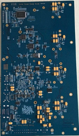
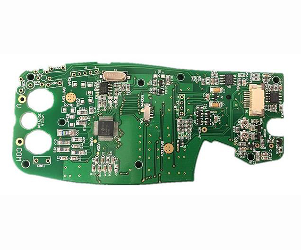
Three categories of PCB reinforcement materials
PCB circuit boards are indispensable for machinery and electrical equipment, as well as an indispensable carrier for software development. Different machinery and equipment have different PCB materials. For rigid printed circuit boards (RPCB) ) Can be divided into many types, according to the common types of PCB board reinforcement materials can generally be divided into the following three
1. Phenolic PCB paper substrate
Since this type of PCB board is composed of paper pulp and wood pulp, sometimes cardboard, V0 board, flame-retardant board and 94HB are also added. Its key material is wood pulp fiber paper, which is pressurized and synthesized by phenolic resin. Kind of PCB board.
The characteristics of this kind of paper substrate are not fireproof, can carry out punching processing, low cost, low price, and low relative density. We often see phenolic paper substrates such as XPC, FR-1, FR-2, FE-3, etc. And 94V0 belongs to flame-retardant paperboard, which is fireproof.
2. Composite PCB substrate
This kind of powder board is also added, with wood pulp fiber paper or cotton pulp fiber paper as the reinforcement material, and at the same time supplemented with glass fiber cloth as the surface reinforcement material. The two materials are made of flame-retardant epoxy resin. There are single-sided half-glass fiber 22F, CEM-1 and double-sided half-glass fiber board CEM-3, among which CEM-1 and CEM-3 are the most common composite base copper clad laminates.

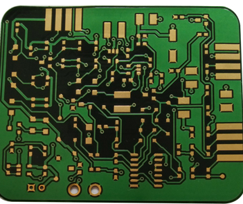
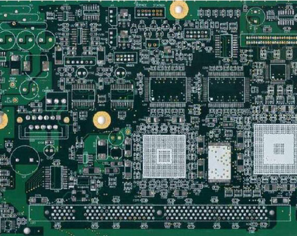
3. Glass fiber PCB substrate
Sometimes epoxy board, glass fiber board, FR4, fiber board, etc. are also added. It uses epoxy resin as a binder, while glass fiber cloth is used as a reinforcing material. This type of circuit board has a high working temperature and is not affected by environmental factors. This type of board is often used in double-sided PCBs. However, the price is relatively more expensive than the composite PCB substrate, and the common thickness is 1.6MM. This type of substrate is suitable for various power supply boards, high-level circuit boards, and is widely used in computers, peripheral equipment, and communication equipment.
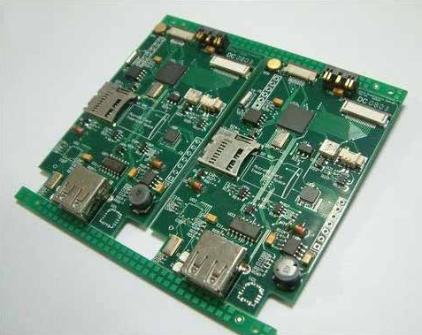
Three reasons for aging of solder joints in PCBA processing
Failure mode of solder joint
The reliability test operation of PCBA processing solder joints includes reliability test test and specific analysis. The purpose of the first level is to evaluate and detect the reliability test level of integrated circuit chip electronic components, and provide data parameters for the reliability design of the entire equipment; and On the other hand, it is to improve the reliability test of solder joints. This requires specific analysis of failed products, finding failure modes, and specific analysis of failure causes. The purpose is to improve and optimize the design process, structural parameters, welding process, etc., and the failure mode of solder joints is based on the prediction of cycle life. Analysis is very critical and is the basis for creating its mathematical analysis model. Next, we will introduce three failure modes in detail.
1. Solder joint failure caused by welding process
Some objective conditions in the welding process and the subsequent unreasonable cleaning process may cause the solder joint to fail. The reliability test status of SMT solder joints mainly comes from the production and installation stage and the putting into use stage. In the production and installation stage, due to the limitations of equipment conditions such as pre-welding preparation, welding stage and post-welding inspection, and the human error in the selection of welding specifications, welding failures such as false welding, solder short circuit and Manhattan conditions are often caused.
On the other hand, in the application stage, in view of the inevitable collisions and vibrations, it will also cause mechanical damage to the solder joint. Withstand thermal-mechanical stress. When the temperature difference is too large, the ceramic and glass parts of the electronic components will cause stress cracks. Stress cracks are an objective condition that endangers the long-term reliability test of solder joints.
At the same time, during the installation stage of thick and thin film hybrid circuits (including chip capacitors), there are often gold and silver corrosion conditions. This is because the tin in the soldering material and the gold and silver in the gold-plated or silver-plated pins produce chemical substances, which in turn reduces the reliability test of the solder joints. Excessive ultrasonic cleaning may also be harmful to the reliability test of solder joints.
2. Failure caused by aging
When the molten solder material comes into contact with a clean substrate, intermetallic compounds (intermetallicCompounds) are generated at the interface. In the aging phase, the microstructure of the solder joints will be coarsened, and the IMC at the interface will continue to grow. The failure of solder joints depends in part on the growth kinetics of the IMC layer. Although the intermetallic chemical substance at the interface is a sign of good welding, as its thickness increases during the putting into use stage, it will cause micro-cracks or even breakage in the solder joint.
When its thickness exceeds a certain critical point, the intermetallic chemical substance will exhibit brittleness. In view of the thermal expansion mismatch between the various materials that make up the solder joint, the solder joint will experience periodic strain during the putting into use stage. When the variable is large enough, it will cause failure. Studies have shown that the addition of trace rare earth element lanthanum to the Sn60/Pb40 solder alloy will reduce the thickness of the metal chemical substance, thereby increasing the thermal fatigue life of the solder joint by 2 times, and significantly improving the reliability test of the surface mount solder joint.
3. Failure caused by thermal cycling
When the electronic components are put into use, the regular breaking of the power supply circuit and the regular change of the working temperature will make the solder joints bear the temperature cycle process. The thermal expansion mismatch between the packaging materials will cause stress and strain in the solder joints. If in SMT, the coefficient of thermal expansion (CTE) of the chip carrier material A1203 ceramic is 6&TImes;10-6 degree Celsius-1, while the CTE of the epoxy resin/glass fiber substrate is 15&TImes;10-6 degree Celsius-1. When the temperature changes, the solder joints will bear the corresponding stress and strain. Generally, the strain borne by the solder joint is 1% to 20%. In the THT process, the flexible pins of electronic components will absorb most of the strain caused by thermal mismatch, and the strain that the solder joint bears is not large. In SMT, the strain is basically borne by the solder joints, which will cause the initiation and expansion of cracks in the solder joints, and finally fail.