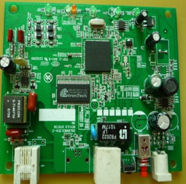
PCB design errors and PCB quality acceptance standards
PCB design error
1. The PCB process has no edges and process holes, which cannot meet the clamping requirements of SMT equipment, which means that it cannot meet the requirements of mass production.
2. The PCB shape is abnormal or the size is too large or too small, which also cannot meet the clamping requirements of the equipment.
3. There is no optical positioning mark (Mark) around the PCB and FQFP pads or the Mark points are not standard. For example, there is a solder mask around the Mark point, or it is too large or too small, resulting in too small contrast of the Mark point image and frequent alarms of the machine. Work.
4. The size of the pad structure is incorrect. For example, the pad spacing of chip components is too large or too small, and the pads are asymmetrical, resulting in skew, tombstone and other defects after the chip components are soldered.
5. There are via holes on the pads, which will cause the solder to melt and leak to the bottom layer through the via holes during soldering, causing too little solder in the solder joints.
6. The size of the pads of the chip components is asymmetric, especially the ground wire and part of the wire are used as the pads, so that the pads at both ends of the chip components are heated unevenly during reflow soldering, and the solder paste melts successively to cause tombstones. defect.

7. The IC pad design is incorrect. The pad in the FQFP is too wide, causing bridging after soldering, or the back edge of the pad is too short to cause insufficient strength after soldering.
8. The interconnection wires between IC pads are placed in the center, which is not conducive to the inspection after SMA welding.
9. The IC has no auxiliary pads during wave soldering, which causes bridging after soldering.
10. The PCB thickness or the IC distribution in the PCB is unreasonable, and the PCB is deformed after soldering.
11. The design of the test point is not standardized, so that ICT cannot work.
12. The gap between SMDs is incorrect, and it is difficult to repair later.
13. The solder mask and the character map are not standardized, and the solder mask and the character map fall on the pads, causing virtual soldering or electrical disconnection.
14. Unreasonable board design, such as poor processing of V-shaped grooves, causing PCB deformation after reflow.
One or more of the above-mentioned errors will appear in poorly designed products, which will affect welding quality to varying degrees. Designers do not know enough about the SMT process, especially not knowing the "dynamic" process of components during reflow soldering is one of the reasons for poor design. In addition, the neglect of the participation of craftsmen in the early design stage and the lack of manufacturability design specifications of the enterprise are also the reasons for poor design.
What aspects does the PCB quality acceptance standard include?
PCB quality acceptance standards
PCB quality acceptance should include design, process, and comprehensive approval. Generally, trial welding, sample sealing, and batch supply should be done first, including the following aspects:
1. Electrical connection performance. Usually self-inspected by the PCB manufacturer, the test instruments used are:
Light board tester (continuity tester). It can measure the on and off of the connection, and whether the logic relationship of the multilayer board including the metallized hole is correct.
Automatic optical tester for pattern defects. You can check out the comprehensive performance of the PCB, including lines, characters, etc.
2. Manufacturability. Including appearance, smoothness, flatness, cleanliness of characters, resistivity of vias, electrical properties, heat resistance, solderability and other comprehensive properties.
There should be no residual flux, glue and other oily traces on the PCB surface. There is no short circuit or open circuit.
The non-line conductor (residual copper) must be more than 2.5mm away from the line, and the area must be ≤0.25mm2
The drilling is not allowed to have excessive drilling, missing drilling, deformation, and through-hole impermeability.
It is not allowed to warp the circuit and the pad; the circuit is not allowed to be exposed to copper and tin.
PCB is not allowed to break; if the board requires VCUT, its depth must be deep into 1/3 of the board thickness.
The actual circuit width shall not deviate from the original design width by ±20%; the shape tolerance is ±0.15mm; the convexity or unevenness of the edge of the substrate is less than or equal to 0.2mm.
The offset of the solder mask oil silk screen should not exceed ±0.15mm; the surface of the solder mask oil is not allowed to have fingerprints, water lines or wrinkles.
The text on the component surface must not be damaged or unrecognizable; the painted area on the pad must be ≤10% of the original area.
The degree of PCB deformation, bending and warping is less than or equal to 1% of the diagonal length of the substrate.
After the PCB quality is accepted, the vacuum packaging machine is generally used for the vacuum packaging of the product. The purpose is to prevent dust and moisture, so as to extend the storage period. Generally, after 1 to 2 years of storage, its solderability can still be Keep it fine.
What are the common PCB design errors and their causes and PCB quality acceptance standards?