Abstract: To successfully use today's SOC, board-level and system-level designers must understand how to best place components, layout traces, and use protective components.
They are called digital cellular phones, but they contain more analog functions than the so-called analog cellular phones before. In fact, any system that needs to process continuous state values (such as voice, image, temperature, pressure, etc.) will have its analog function, even if the word digital appears in its name. Today’s multimedia PCs are no exception. They have voice and video input and output, urgent temperature monitoring of the heating central processing unit, and high-performance modems. These systems are also items on the list of mixed signal functions. Also more and more.
The trend of the two systems brings new challenges to people who design hybrids. The volume and weight of portable communication and computing devices continue to decrease, but their functions continue to increase. The desktop system continues to improve the central processing unit capacity and the speed of communication peripherals. To be sure, it is quite difficult to design modern digital circuit boards while avoiding ringing, noise-induced errors, and ground potential bounce. However, when you add those analog signal lines that are susceptible to noise close to square-wave excitation digital data lines, the problem becomes more serious.
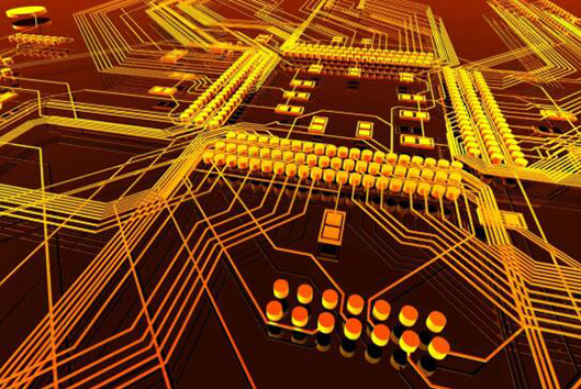
At the chip level, the current SOC (system on chip) requires expertise in logic circuits, analog circuits, and thermodynamic design. To successfully use these ICs, board-level and system-level designers need to understand how to best place components, route traces, and use protective components.
This article describes the common pitfalls in current mixed-signal system design and provides some guidelines to clear or remove them. However, before discussing specific issues and making proposals, it will be of great help to take a detailed look at how the two trends in system design-miniaturization and high-speed-affect these issues.
1. "High-speed" trend
Comparing the specifications of a mid-range PC in 1999 with those five years ago, its central processing unit speed has increased by about an order of magnitude, and the current consumed by the CPU has also increased by about an order of magnitude. When you combine high speed with high current, the "di/dt" part of the relationship of V=L (di/dt) is greatly improved. In fact, the half-inch-long ground wire in the circuit board may induce a voltage of more than 1 volt on it. For the converter, the ground potential reference line will induce voltage, which may cause the operation to stop.
To achieve these higher speeds, ICs are designed and manufactured with deep sub-micron dimensions (for example, 0.35μm). Although this reduces the geometric size and results in much faster performance, it also makes these devices more likely to cause latch-up and damage caused by transients. Moreover, these devices also require tighter energy management to comply with increasingly stringent allowable voltage ranges.
The current 10/100Ethernet network interface card (NIC) is a good example. The original 10Base-T chip is a large-size CMOS device, which is relatively insensitive to overvoltage damage. However, the new chip uses a line width of 0.35μm, which is very sensitive to lock-up and failure due to transients-transients caused by electrical energy and lightning.
Modern servers, with SMP (Symmetric Multiprocessing Capability) architecture, and CPUs operating at frequencies of 500MHz or above are good examples of energy distribution challenges. You cannot simply build a 5V power supply and route the wiring to the corresponding bus. Switching with a current of up to 20A or 30A at 500MHz, it requires actually an independent converter for each point-of-use, plus a larger primary voltage source for all of these converters Supply power.
The trend requires hotswap capability, which means you need to be able to insert or remove circuit boards in the current system. This is also to predict that there will be transients. In this way, both the inserted board and the motherboard must have proper protection.
Both miniaturization and high-speed trends have their own unique problems. For example, high-current energy distribution is not a big problem for small, portable, and handheld devices. For desktop computers and servers, extended battery life will not be a problem. However, damage caused by locking and transients becomes a problem in both of these areas.
2. The trend of "miniaturization"
Comparing the 1999 cellular phone with the product five years ago, the number of chips is much smaller, the weight and volume are greatly reduced, and the battery life is greatly extended. In this process, the main factor is the great progress in mixed-signal IC solutions. However, with the reduction of chip geometry, the spacing of the wiring on the circuit board is getting closer, and the laws of physics are beginning to appear.
Parallel traces are getting closer and closer to produce larger and larger parasitic capacitive coupling, and this is simply the result of the inverse relationship with the square of the distance. There used to be only a few traces of space, and now many traces are included. As a result, Even capacitive coupling between non-adjacent traces can pose a problem.
Cellular phones, determined by their nature, are devices that are held and used by people. On low-temperature days, you are walking around on the carpet, then pick up the cell phone, and then "pop"-this sends a high-voltage, electrostatic discharge (ESD) pulse to the device. Without proper ESD protection, one or more ICs may be damaged. However, adding external components to protect against ESD damage will go against the trend of miniaturization.
Another issue is energy management. Cell phone users want the longer the interval between two charges of the battery, the better. This means that the DC-to-DC converter must be very efficient. Switching technology is its answer, but in this case, the converter has also become its own potential noise source. Therefore, the converter must be carefully selected, placed, and interconnected. Also, since volume is a factor that cannot be ignored, one should choose the kind of components that can use passive components with the smallest physical size. If you use a linear regulator, you should choose an ultra-low dropout type that can maintain the output at the minimum battery voltage. This allows the battery to discharge as much as possible before it no longer provides enough power.
3. Locking and transients
Transients from line width to deep sub-micron ICs deteriorate the susceptibility to overvoltage conditions, which means you have to be smarter to protect these devices without affecting their performance.
In a protection input, any protection component must appear as a high impedance circuit under normal operation. It must be loaded with the smallest possible capacitive load, for example, if it is to add a small effect to the normal input signal. However, at the moment of overvoltage, that same device must become the main path of the transient energy, leading it away from the input of the protected device. Also, the withstand voltage of the protection device should be higher than the maximum allowable voltage on the pin it protects. In the same way, its clamping voltage should be low enough to prevent damage to the protected device. This is because in transient conditions, the voltage on the input will be the clamping voltage of the protection device.
Previously, transient voltage suppression (TVS) diodes effectively clamped transients on printed circuit boards. Traditional (TVS) diodes are solid-state PN junction devices that work well with voltages as low as 5V. They have fast response time, low clamping voltage, high current surge capability-all the desired characteristics. However, the problem with the traditional TVS diode is that it will lift its head if it is below 5V. Here, the avalanche technology they use is an obstacle. To achieve Stand-off voltage below 5V, a high degree of doping (1018/cm-3 or above) is required. This, in turn, will cause higher capacitance and leakage current, both of which will impair high performance. Traditional TVS diodes have voltage-dependent capacitance, which increases as the voltage decreases. For example, at 5V, a typical ESD protection diode will have a junction capacitance of 400pF. We can imagine that if such a capacitive load is applied to the input node of a 100Base-TEthernet transmitter or receiver, or applied to the universal serial bus (USB) input, what will happen. Moreover, these are exactly the types of circuits that are most in need of transient protection.
In the case of voltages below 5V, traditional TVS diodes are not really an option. But this does not mean that you have no choice. A new technology jointly developed by the University of California, Berkeley and Semtech (NewburyPark, California) provides transient and ESD protection down to a working voltage of 2.8V. You can choose one among a series of TVS devices, with suitable capacitance, stand-off voltage, and clamping voltage to meet the requirements of your own system. After that, we must also consider where the device should be placed on the board and how to wire the circuit board.
The parasitic inductance in the protection path can cause high voltage overshoot and damage the IC. This is especially true for fast rise time transients, such as ESD. The transient induced by ESD, according to the definition of IEC1000-4-2, will reach its peak value in less than 1 nanosecond (ns). Calculated based on the trace inductance of 20nH/inch, four 1-inch traces from a 10A pulse will cause an overshoot of 50V.
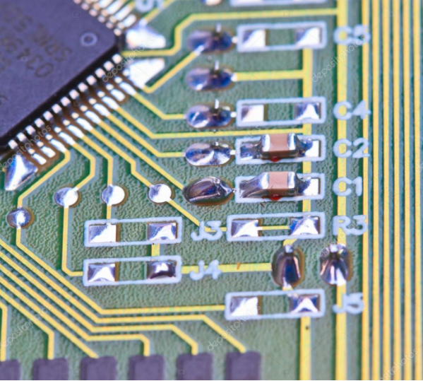
You must consider all possible inductive paths, including the ground return path, the path between the TVS and the protection circuit, and the path from the connector to the TVS device. Also, TVS devices should be placed as close to the connector as possible to couple transients to other traces nearby.
A 10/100Ethernet board is a subsystem that needs transient protection. The devices used in Ethernet switches and routers are exposed to high-energy, lightning-induced transients. The depth submicron IC used is extremely sensitive to overvoltage lock-up in design. In a typical system, the twisted pair interface used by each port consists of two different signal pairs-one pair for the transmitter and the other pair for the receiver. The transmitter input is usually the most susceptible to damage. There will be a different lethal discharge in a line pair, and it will be capacitively coupled to the EthernetIC through a transformer.
There is a situation where the signal frequency is very high (100Mbit/s) and the power supply voltage is low (typically 3.3V), the protection device must have a very low capacitive load, and its stand-off voltage is much lower than 5V. There is another case in which parasitic inductance in the protection path can cause a large voltage overshoot. In order to maximize efficiency, the wiring of the circuit board should be such that the path between the protector and the protected circuit must be minimized, and the path length between the RJ45 connector and the protector must also be minimized.
4. Heat exchange/plug and play
More and more systems are designed to allow plug boards or plugs to be inserted and removed at any time while the system is still powered on. Those plug-in boards or plugs will be inserted into or unplugged from sockets that carry signals, power cords, and ground wires, and there is a high chance of transients. In addition, the system can dynamically adjust its power supply to adapt to sudden increases or decreases in current load.
Cellular phones or other portable electronic devices are accidentally plugged into or unplugged from the self-charging system during charging. This also produces transients. Here, in addition to transient protection, energy management is also required to adapt to sudden increases or decreases in current load.
The USB interface is designed to improve a high-speed serial interface between the desktop system and peripheral devices. Also, there is a voltage supply line on the UB interface, which can be used to supply power to connected peripheral devices. If no load is plugged into the USB socket, it is an open socket. The ESD pulse discharge induced by the human body static electricity on the socket will be conducted to the circuit board and easily damage the USB controller.
You must ensure that in this high-speed bus, both the data line and the power line are protected. Moreover, although energy management has been written into the USB specification, ESD protection has not yet been provided.
TVS devices can be used to provide appropriate ESD protection. The placement of components and the length of the path are still important design issues. The same layout guide should be carefully consulted. Make sure that the path between the TVS and the protected line be shortened, and make sure that the TVS device is as close as possible to the port connector.
According to the needs of the USB specification, a solid-state circuit energy distribution switch should be used for energy management. In the PC host, they provide short-circuit current protection and error reporting to the controller IC. In USB peripherals, they are used for port switching, error reporting and supply voltage ramp-down control.

5. Energy distribution
If you compare the change in the amount of PC current with that of 10 years ago, the magnitude of the increase is really astonishing. Coupled with the substantial increase in clock frequency, PCs and servers are in a very high di/dt environment. For example, if L is 2.5μH and C is equal to 4*1500μF, the transient on the load is of the order of 200mV peak-to-peak, and the recovery time is 50 microseconds. What makes the problem more complicated is that the CPU enters a sleep mode and then wakes up quickly. The transients generated are in the range of 20 to 30A per microsecond, which becomes a headache for energy management.
From the perspective of the converter, the value of di/dt influences the choice of output capacitor, more specifically the equivalent series resistance (ESR) and equivalent series inductance (ESL) of the capacitor. Converters operating at low frequencies need a large capacitance to store the charge between two working cycles, which requires the use of electrolytic capacitors. Although these electrolytic capacitors have a large capacitance, they also have large ESR and ESL, both of which are against the intention of the designer. In addition, electrolytic capacitors are large in size and are not suitable for surface mount technology and compact packaging.
There is an alternative way to reduce the value of ESR and ESL, simplify the production process, and reduce the actual volume. The method is to use a slightly higher frequency converter, you can choose ceramic capacitors instead of electrolytic capacitors, and get the above advantages. At the same time, by adopting the solution of multi-phase converters, you can even share the load demand. Each converter requires less input capacitance while providing the same total current capacity. Another advantage is that it reduces the input ripple current. In the single-phase conversion scheme, the input ripple current is equal to half of the output ripple current. Therefore, for a 20A system, the input ripple current is 10A. However, for a four-phase converter solution, for example, this output current will be divided equally among the four converters. Now each power supply is 5A, and their input ripple current is 2A. This allows the use of smaller and cheaper input capacitors.
DellComputers (RoundRock, Texas) has developed a discrete, multi-phase pulse width modulation (PWM) controller and reverse DC-to-DC converter for its high-speed computer and server series. Its design is to meet the urgent power/energy management requirements of Intel's advanced PentiumCPU. The circuit has since been integrated by Semtech at Dell's request. Multi-phase controller and converterAfter the solution, you have to pay special attention to the wiring problem of the circuit board. The high current switching at high frequency will affect the voltage difference of the ground plane.
The high-current part of the circuit should be routed first. You should use a ground plane, or you should introduce an isolated or semi-isolated ground plane area to limit the ground current from entering a specific area. The loop formed by the input capacitor and the high-side and low-side driver output FETs contains all the high-current, fast-transient switching. The connection should be wide or wide and short or short to reduce loop inductance. Doing so will reduce electromagnetic interference (EMI), reduce the current injected into the ground, and minimize the source ringing to obtain a more reliable gate circuit switching signal.
The connection between the junction of the two FETs and the output inductor should be a wide track and at the same time as short as possible. The output capacitor should be placed as close as possible to the load. The fast transient load current is provided by this capacitor, so the connecting wire should be wide and short to minimize inductance and resistance.
The controller is best placed in a quiet ground plane area to prevent the pulse current in the input capacitor and FET loop from flowing into this area. The high and low ground reference pins should return to the ground very close to the control amplifier package. The small signal analog ground and digital ground should be connected to the ground of one of the output capacitors. Never return to the ground inside the input capacitor/FET loop. The current sense resistor loop should be kept as short as possible.
6. Work smart
Although the above examples illustrate some methods that can predict and avoid certain pitfalls of mixed-signal systems, they are by no means exhaustive. Each system has its own challenges, and each designer has its own unique obstacles to jump over. Whether dealing with more difficult protection or stricter energy management, choosing the right components is the first thing to do. In terms of challenge converters, converter controllers and TVS protection devices, there is a wide range of options. Placing them in the right place on the circuit board will show the difference in energy management and protection. Well-thought-out wiring and ground plane configuration are the key issues in the third aspect. TVS for low-voltage circuits
When the voltage is lower than 5V, the traditional PN junction TVS actually does not work at all. However, there is an enhanced punch-through diode (EPD) developed by the University of California, Berkeley and Semtech.
Unlike the traditional PN structure of avalanche TVS diodes, this EPD device uses a more complex n+p+p-n+ four-layer structure. It uses light doping in the p+ and P- layers to prevent the reverse-biased n+p+ junction from entering an avalanche state.
The npn structure was chosen instead of the pnp structure because of its higher electron mobility and improved clamping characteristics. By carefully fabricating the P-base region, the resulting device has excellent leakage, clamping and capacitance characteristics in the voltage range of 2.8V to 3.3V.
7. Pentium with great appetite
Intel’s Pentium II specification requires that the current be increased from 5A to 20A within 500ns, and the conversion rate is 30A per microsecond. The Semiteck SC1144 multi-phase PWM controller is more capable than the task requires. It provides control of up to four reverse DC-to-DC converters to get the required speed and accuracy. The built-in 5-bit DAC allows the output voltage to be programmed output, from 1.8 to 2.05V in 50mV increments, and from 20 to 3.5V in 100mV increments.
This multiphase technology produces four precise output voltages separated by a 90-degree phase shift. Then, the four digitally phase-shifted outputs are summed together to obtain the required output voltage and current capacity.
With each converter operating at 2MHz, designers can use ceramic capacitors instead of electrolytic capacitors, and get the benefits of small size, surface mountability, and lower ESR and ESL.