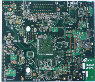
In short, printed circuit boards, also known as PCBs, enable all electronic devices to function as expected. Therefore, when there is a problem with the printed circuit board. Electronic equipment may not operate as expected. The printed circuit board problem is a major challenge for manufacturers, because many things can go wrong. Especially in the multi-layer PCB manufacturing process. Listed below are 7 problems in the manufacturing process of multilayer PCBs.
By understanding these issues, as a designer, you will take these issues into consideration when building a printed circuit board, hoping to avoid them and subsequently cause damage to your printed circuit board.
design
When designing multilayer printed circuit boards, problems related to bowing and twisting may arise. Bending and twisting are some of the most common characteristics used to determine PCB flatness. The arc is the cylindrical or spherical curvature of the printed circuit board. On the other hand, distortion is a condition that occurs when the deformation is parallel to the diagonal of the printed circuit board.
There are several steps for a multi-layer correct PCB service provider. Fortunately, there are various PCB manufacturing companies that can take steps to avoid bending and twisting. First of all, multi-layer PCB manufacturers need to use appropriate parameters when pressing multi-layer PCBs to reduce the stress on the printed circuit board. Second, they need to avoid mixing materials from multiple suppliers. Third, the materials used should comply with RoHS guidelines. As a PCB manufacturer, you also need to use or adopt a horizontal oven during the curing process to avoid problems related to PCB bending and twisting.
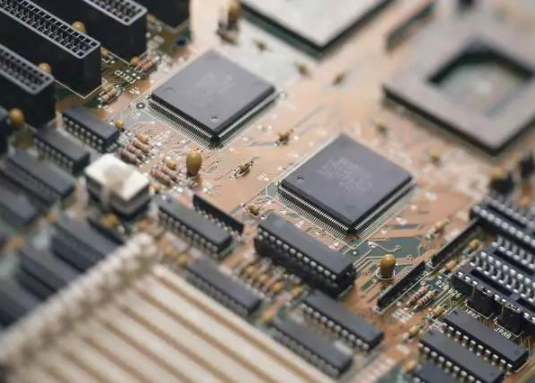
Press multilayer PCB

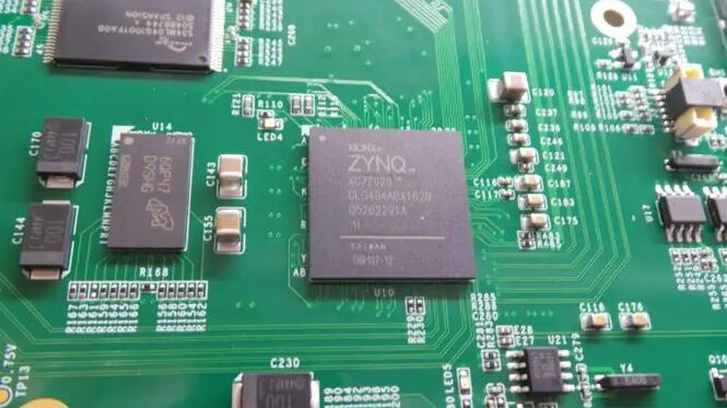
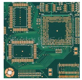
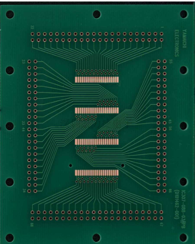
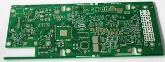
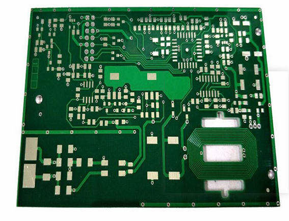
Multilayer printed circuit boards are those that contain multiple single-layer counts and therefore need to be stacked. Laminate is to lay out the insulating layer and the copper layer before the PCB layout design to make a printed circuit board.
In the manufacture of multilayer printed circuit boards, there are challenges in laminating the insulating layer and copper together. Most multilayer printed circuit board manufacturers often encounter difficulties when pressing the components of the multilayer printed circuit board together.
In order to ensure that the stacking process of multilayer printed circuit boards goes smoothly, in addition to using the best laminate materials, manufacturers also need to ensure that they use the most suitable machine for the job.
The choice of substrate
Printed circuit board materials have two basic uses. First, they conduct electricity, and second, they provide insulation between conductive copper layers. Therefore, it is easy to understand why the choice of substrate material is critical to the failure or success of a printed circuit board. In addition to affecting the thermal behavior of the PCB. The documents you use on the PCB also affect the mechanical and electrical characteristics of the PCB.
1. Dielectric constant
Because most of the printed circuit board functions are determined by the substrate material. Then it means that substrate materials with high-frequency characteristics need to be applied to high-frequency and high-speed PCBs. However, high-frequency substrate materials must satisfy a small and stable dielectric constant.
2. Substrate characteristics
In addition, the substrate material must also perform well in terms of heat resistance. Stability, impact strength, chemical resistance and manufacturability. It is important to ensure that substrate materials used for high-speed and high-frequency printed circuit boards must have low moisture absorption or be composed of low moisture absorption. Copper foil also needs to meet high peel strength.
3. Insulation
FR4, also known as FR-4, is one of the most versatile low-cost multilayer substrate materials and is known for providing excellent performance. FR-4 material provides some of the best electrical insulation with high dielectric strength.
Multilayer PCB manufacturing-resin penetration manufacturing
The resin plugging process is a standard process in the entire printed circuit board industry, especially in high-frequency products that require large thickness and high-level count. Recently, the application of resin plugging technology has become more and more extensive, and it has been widely used in HDI panels. If you want to solve or eliminate the problems that cannot be solved by pressure filling or green oil plugging resin, it is best to use resin for plugging.
When manufacturing multilayer printed circuit boards, resin plugging is a problem faced by most manufacturers. However, the best way to solve such problems is to use a vacuum plug machine.
Resin blockage is a preventive measure designed to ensure that through holes are protected from accidental flow of solder material, especially during soldering and assembly. The main purpose of resin, especially when manufacturing printed circuit boards, is to clamp fibers together and protect them from external factors.
Dense heat dissipation hole manufacturing
When manufacturing printed circuit boards, you may encounter problems related to heat dissipation. Heat dissipation is a method of heat transfer. When an object that is hotter than other uses is placed or placed in an environment where the heat of the hotter component is transferred to the environment of the colder object, heat dissipation occurs. Heat dissipation occurs through a variety of methods, mainly through convection, conduction, and radiation.
Problems related to heat dissipation are a problem faced by many printed circuit board manufacturers. However, to eliminate intensive heat dissipation, it is best to use the best or recommended heat dissipation material, such as aluminum.
Multilayer PCB manufacturing-back drill production
Back drilling is one of the best manufacturing techniques, usually used in a large number of high-speed multi-layer printed circuit boards to reduce or minimize the parasitic effects of plated through holes. Back drilling, also known as controlled depth drilling, is a technique that allows you to remove some unused parts, stubs, and copper pipes from the through holes on the circuit board of the printed circuit board.
In addition to improving signal integrity and reducing the difficulty of manufacturing printed circuit boards, back drilling also reduces noise interference on printed circuit boards. When it comes to the manufacture of multilayer printed circuit boards. Back drilling is a major challenge faced by many manufacturers. Some of the most likely back-drilling challenges include hole cleaning. Barite depressions, stuck tubes, circulation losses and shale instability.
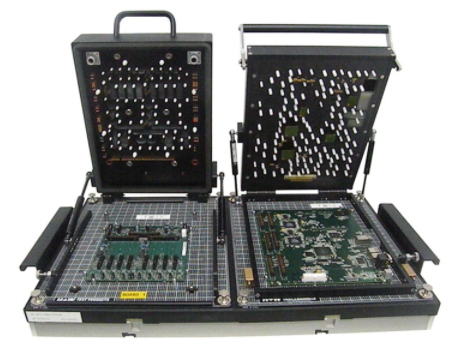
Multilayer PCB manufacturing-testing
In the PCB development cycle, the testing phase of the printed circuit board is an indispensable part. In the entire printed circuit board manufacturing process. Testing printed circuit boards can help save money and prevent problems or difficulties in the final production run.
Unfortunately, when it comes to multilayer manufacturing. Most PCB manufacturing companies have failed when using the best PCB testing methods. Some of the best and recommended printed circuit board testing are bare board testing, in-circuit testing, functional testing, and assembly-level testing. Testing, especially in multilayer printed circuit boards, can identify any technical defects in the printed circuit board.