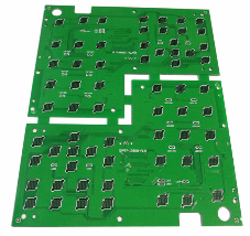
Causes and solutions of PCB technology negative film deformation
reason:
(1) Poor temperature and humidity control
(2) The temperature of the exposure machine rises too high
solution:
(1) Generally, the temperature is controlled at 22±2°C, and the humidity is controlled at 55%±5%RH.
(2) Use a cold light source or an aerator with a cooling device, and constantly replace the spare membrane
PCB technology's negative film deformation solution
Negative film distortion correction process:
1. Change the hole position method
In the case of mastering the operating technology of the digital programmer, first, compare the negative film with the drilled test board, and measure the two deformation amounts of length and width.

On the digital programmer, the position of the hole is extended or shortened according to the amount of deformation, and the drilled test board with the extended or shortened hole position is used to adapt to the deformed negative film. This method eliminates the tedious work of splicing films and ensures the completeness and accuracy of graphics.
2. Hanging method
In view of the physical phenomenon that the negative film will change with the change of environmental temperature and humidity, put the negative film in a sealed bag before copying the negative film and hang it for 4-8 hours under working environment conditions, so that the film will be deformed before copying. Make the film very small after copying.
3. Splicing method For patterns with simple lines, wide line width, large spacing, and irregular deformation, the deformed part of the negative film can be cut, and then re-spliced on the hole position of the drilled test board before copying
4. PCB pad overlap method
Use the hole on the test board to expand it to the size of the pad, and remove the deformed line segment to ensure the minimum loop width technical requirement.
5. Texture method
Enlarge the graphics on the deformed film proportionally, and then reposition the printing plate
6. Shooting method
Use the camera to zoom in or out of the deformed figure.
PCB technology's negative film deformation solution
Notes on these related methods
1. Splicing method:
Application: The coating film lines are less dense, and the coating film deformation of each layer is inconsistent; it is especially suitable for the deformation of the solder mask and the multi-layer power grounding film;
Not applicable: The wire density of the negative film is high, and the line width and spacing are less than 0.2mm;
Note: When cutting, please minimize the damage to the wire, and do not damage the gasket. When splicing and copying, attention should be paid to the correctness of the connection relationship.
2. How to change the hole position:
Application: The deformation of each layer is consistent. Line-intensive negatives are also suitable for this method.
Not applicable: The film will not deform uniformly, and the local deformation is particularly serious.
Note: After using the programmer to extend or shorten the hole position, the tolerance hole position should be reset.
3. Hanging method:
Applicable; Film that has not been deformed and prevented from deforming after copying;
Not applicable: deformed negatives.
Note: Dry the film in a ventilated and dark environment to avoid contamination. Ensure that the air temperature is the same as the temperature and humidity of the workplace.
4. Pad overlap method
Applicable: The graphic lines should not be too dense, and the line width and spacing should be greater than 0.30mm;
Not applicable: Especially users have strict requirements on the appearance of printed circuit boards;
Note: After overlapping, the PCB pad is oval, and the line and the halo on the edge of the pad are easily deformed.
5. How to take pictures
Application: PCB film has the same deformation rate in the length and width directions. If it is inconvenient to use bulky drilling test boards, only silver salt film should be used.
Not applicable: The length and width of the film are deformed differently.
Note: When shooting, the focus should be accurate to prevent distortion of the lines. The loss of film is great. Normally, many adjustments must be made to obtain a satisfactory circuit pattern.