Today's society has higher and higher requirements for electronic engineers, who can not only design digital circuits, but also have the ability to handle analog circuits and PCB layout. Now let me talk about the things that must be paid attention to in the PCB layout of this kind of board that contains both digital and analog circuits.
In this kind of board with AD circuit, there are generally two situations:
a. Digital circuits and low-frequency analog circuits (usually sound design circuits and radio frequency circuits)
b. High-power motor circuits and relay circuits in digital circuits and analog circuits.
Need to pay attention to three basic principles in this circuit design:
1. Appropriate use of the division of digital ground and analog ground;
2. The current returns to the power supply through the smallest loop;
3. Have a reference ground plane.
If you do not pay attention to the division of digital ground and analog, directly divide into two parts, it will cause a variety of unexpected situations, and even greater noise after division, so you need to be careful when using ground plane division Considerations. If the current loop in the circuit is too large, high ground inductance will be generated in the high-frequency circuit, and at the same time, the analog circuit will receive greater interference. There is also a situation where the two ground planes are not on the same reference plane. When this happens, knowledge of radio frequency and microwave can be known, so that it is easy to construct a dipole antenna.
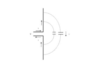
Dipole antenna model
I believe everyone has corresponding opinions on the treatment of digital ground and analog ground, such as single-point grounding, multi-point grounding, star grounding, floating ground, and so on. For the connection of analog ground and digital ground, methods such as inductors, magnetic beads, and 0 ohm resistors are commonly used.
First of all, what is commonly used is the separation of digital and analog power. But you can't simply divide it and everything will be fine. There are also things to pay attention to when the analog ground and digital ground are divided.
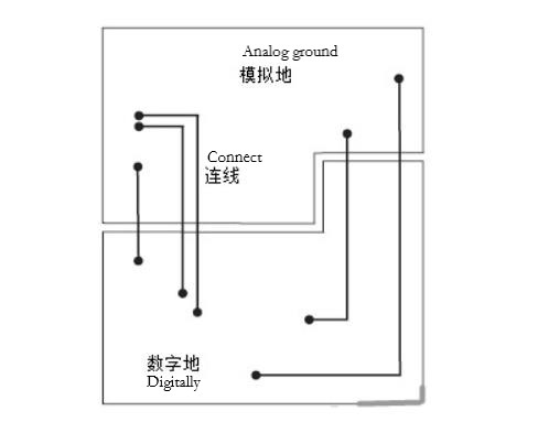
Connection situation of analog ground and digital ground one
In this case, if you do not pay attention to the interconnection when doing the PCB layout, the current flow loop will be enlarged. In the high frequency circuit, the large current loop will produce high ground inductance, which will cause the analog circuit Great influence and interference. At this time, we often use single-point grounding, differential line or star grounding to reduce loops. If the wiring between the analog circuit and the digital circuit is very important, this requires a "bridge" concept through the bridge and the differential line, Reduce interference. As shown below:
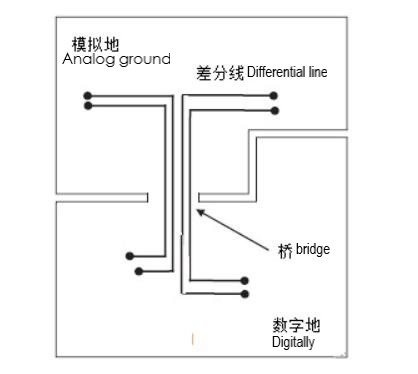
Analog ground and digital ground connection situation 2
When using analog ground and digital ground to lay out separately, it must be noted that the analog signal must be arranged in the analog part of the board, and the digital signal must be arranged in the digital part of the board, and there are these two parts on all layers. In this case, the digital return current will no longer exist in the analog part of the ground plane.
One of the inevitable problems with the partitioning method is that the analog signal traces have to pass through the digital part of the board (and vice versa). In this case, the partition processing is difficult to be effective. Therefore, for all PCB layouts, the focus is Use a single ground plane, divide it into analog and digital parts, and then apply signal arrangement principles.
With the maturity of large-scale integrated circuit technology, a large number of integrated IC chips flood into our electronic design career. When we do PCB lay out, we will encounter this situation: an IC chip has an analog terminal and a digital terminal. The good point is that most of the IC product manuals explain the grounding method relative to a single PCB, and it is usually the manufacturer’s own evaluation board. According to the connection method specified by the manufacturer, there will generally be no problems. This requires us to watch the chip patiently. The data sheet is out. Generally, the PCB ground layer is divided into an analog layer and a digital layer, put the analog ground (AGND) and digital ground (DGND) pins together, and connect the analog and digital ground layers at the same point. The chip forms the star ground point of the system. As shown below:
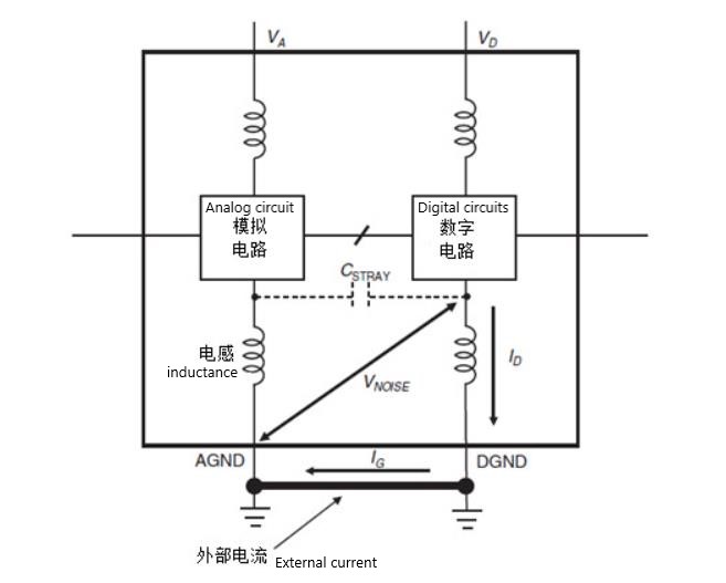
As can be seen from the above figure, all noisy digital currents flow through the digital power supply to the digital ground plane, and then return to the digital power supply to isolate the sensitive analog part of the circuit board. The analog and digital ground planes form the star grounding point of the system when the IC chip intersects. This method is generally effective in using a single PCB and a single IC system, but it is not very suitable for multiple IC chip systems. If there are multiple such chips on a PCB, if this method is adopted, the analog and digital grounding systems are converged at each converter on the PCB, forming many ground loops, thus losing their due advantages. Under normal circumstances, the analog ground and digital ground are used as close as possible to lay out, as shown in the following figure:
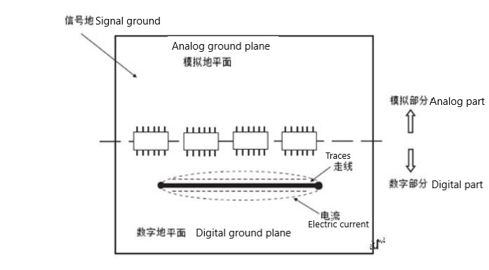
The connection method commonly used by the company's big cow for this situation is: the analog and digital ground planes should be fixedly connected under all ADC and digital-to-analog converter (DAC) chips. The AGND and DGND pins should be connected to each other and connected to the analog ground plane, while the analog and digital ground planes should be separately connected back to the power supply. The power supply should enter the digital partition circuit board, and directly supply power to the digital circuit, and then supply power to the analog circuit after filtering or adjustment. In this way, only the digital ground plane should be connected back to the power source.
Finally, I borrowed a sentence from a revolutionary veteran: "The revolution has not yet succeeded, and comrades still need to work hard." Hope that on the road of PCB lay out and EMC, more and more people will "search up and down"!