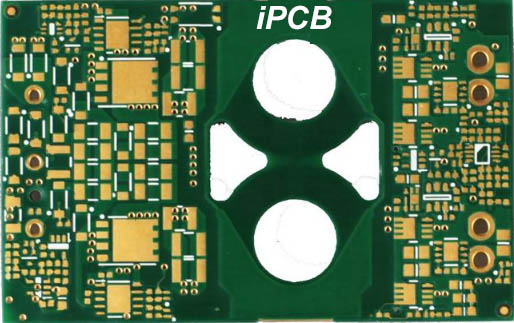
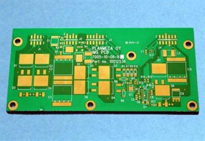
An improved stepped PCB board production process, which is characterized in that it includes an upper substrate, at least one middle substrate and a lower substrate. The process flow is as follows: (1) Cutting: the upper substrate, the middle substrate and the lower substrate are cut according to the requirements. Need to be cut to size; (2) Inner layer: the lower surface of the upper substrate, the upper surface of the lower substrate and the front and back of the middle substrate are formed by image transfer to form a circuit pattern, and then the unnecessary part of the copper foil is processed by a milling machine Removal to form the required loop pattern; then use a molding machine to fish the middle substrate to create a window corresponding to the position and size on the middle substrate; (3) once drilling: the upper substrate, the middle substrate and the lower substrate Aligning pin holes are drilled on the substrate; (4) Resin printing: The alignment pin holes drilled on the upper, middle and lower substrates are selectively plugged with resin by printing; (5) Pressing: in Place the film between the upper substrate and the middle substrate and between the middle substrate and the lower substrate and stack them one by one, use positioning pins to align them together, and send them into a vacuum laminator to harden and bond the films together to form multilayer PCB board;

Then, at the position where the steps need to be made, the upper substrate is cut at a fixed depth by a forming machine, exposing the upper surface circuit pattern of the lower substrate; (6) Secondary drilling: Drilling on the multilayer PCB board by using different specifications of slot cutters Slot holes of the required size; (7) Plating: Copper is plated on the outer surface of the multilayer PCB board and in the slots through a chemical reaction, so that the slots can conduct between the layers; (8) Dry film : Cover a layer of dry film on the outer surface of the copper multilayer PCB board, and form a circuit image on the outer surface of the copper multilayer PCB board through image transfer; (9) Alkaline etching: useless chemical reaction The copper foil is removed to obtain an independent and complete outer layer circuit; (10) Solder protection: a layer of ink is covered on the outer surface of the multilayer PCB board by printing; (11) Printing: on the multilayer PCB board by printing Corresponding symbols are printed on the outer surface; (12) Forming: The whole piece of multi-layer PCB board is removed from the useless frame, and then chemically cleaned and then sorted into the specified shape and specification.
Know the foundry you are using
After discussing DRC settings, this technique is almost-but not entirely-redundant. In addition to helping you correctly establish DRC rules, knowing which foundry your PCB will be sent to can also provide some additional pre-manufacturing assistance. A good foundry will provide some helpful help and suggestions before you place an order, including how to improve your design to reduce design iterations, reduce problems encountered during final debugging on the test bench, and improve the yield rate of PCBs.
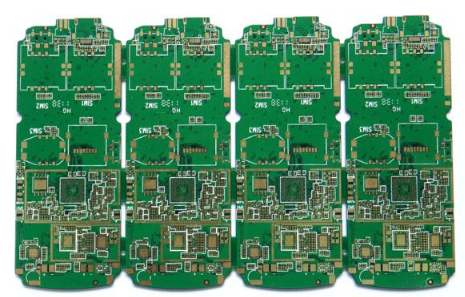
Hugo, a PhD student at Carnegie Mellon University, commented on his knowledge of manufacturers in his blog: "Each manufacturer has its own specifications, such as minimum wire width, spacing, number of layers, etc.. Before starting the design, you should consider Good your own requirements, and then find a manufacturer that can meet your requirements. Your requirements also include the grade of PCB material. The grade of PCB material ranges from FR-1 (paper-phenolic resin mixture) to FR-5 (glass fiber and ring). Oxygen resin). Most PCB prototype manufacturers use FR-4, but FR-2 is also often used in high-volume consumer applications. The type of material will affect the strength, durability, moisture absorption and flame retardancy of the PCB (FR )."
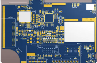
Understanding the manufacturing process of printed PCB and knowing which process and method your manufacturer will use can help you make better design decisions. Visit the supplier of your choice and learn about the manufacturing process for yourself. Make good use of DFM (design for manufacturability) tools before submitting your design to manufacturing.
Summary of this article
If you are thinking about these basic skills and techniques, it means that you are already on the road to a fast, reliable, and professional-quality PCB. Understand the manufacturing process; use DRC and DFM to help you catch negligent design features that may increase foundry costs and/or decrease yield. Then carefully plan the layout of the components to eliminate expensive design features. Use all the design tools provided by CAD tools wisely, including automatic layout and automatic routing, but you must have patience and thoroughness in the setting of the automatic routing device in order to achieve good automatic routing results.
Do not rely on automatic routers for things other than wiring; manually adjust the wire size when needed to ensure that the design carries the correct current. No matter what, you must believe in the flying leads, until all the flying leads disappear 100%, your PCB design can be considered complete. The later PCB proofing and PCB board production can be more time-saving and labor-saving.