This article will discuss four basic (and important) techniques and strategies for both novices and veterans. As long as you pay more attention to these skills in the design, you can reduce the number of PCB design cycles, design time and overall diagnosis difficulties.
Tip 1: Pay attention to the research of manufacturing methods and foundry chemical treatment process
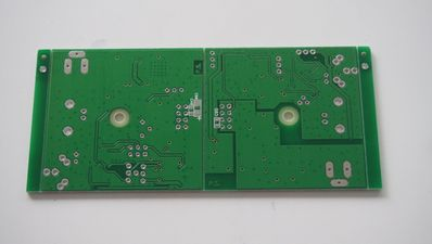
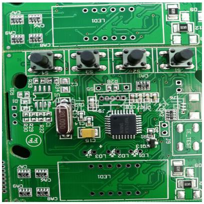
In this era of factoryless IC companies, many engineers really don't know the steps and chemical processing involved in generating PCBs from their design files. This is actually not surprising. This lack of practical knowledge often leads design novices to make more complex design choices that are not necessary. For example, a common mistake made by novices is to design PCB layouts with particularly precise dimensions, that is, to use orthogonal wires that are connected to a tight grid. Finally, it is found that not every PCB processing plant can produce them on site. It is designed to maintain sufficient reliability during the service life.
A factory with these capabilities may not be able to provide the most economical PCB price. Does the design really need to be that complicated? Can PCB layout be designed on a larger grid to reduce PCB cost and improve reliability? Other misunderstandings encountered by design novices include too small via sizes and blind and buried vias. These advanced via structures are the product of powerful tools in the PCB engineer's toolbox, but their effectiveness is highly dependent on specific situations. Just because they are in the toolbox does not mean they should be used.
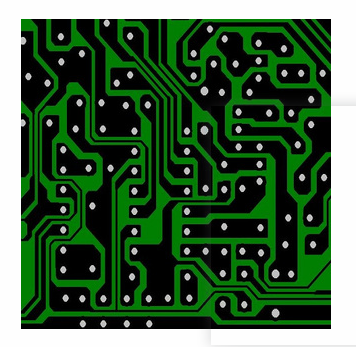
Bert Simonovich’s "Design Notes" blog talked about the aspect ratio of vias: "A via with an aspect ratio of 6:1 can ensure that your PCB can be manufactured anywhere." For most For high-speed PCB design, with a little thought and planning, these HDI features can be completely avoided, thereby saving costs again and improving the manufacturability of the design. The physics and fluid dynamics required for copper plating of these ultra-small or single-port vias are not what all PCB factories are good at. Remember, a bad via can ruin the entire PCB; if you have 20,000 vias in your design, then you have 20,000 chances of failure. Including unnecessary HDI via technology, then the probability of failure will only increase.

Tip 2: Believe in the flying line
Sometimes drawing schematics when designing a simple PCB seems to be a waste of time, especially after you have done one or two designs. But for novice designers, drawing schematics can also be a daunting task. Skip the schematic is a tactic often adopted by novices and moderately proficient people. But we must resist this strong desire. Starting to develop your layout from a complete schematic that you can use as a reference will help ensure that your layout connections are fully completed. Some explanations are given below.
First of all, the schematic is a visual description of the circuit, which can communicate information on many levels. The sub-sections of the circuit can be drawn in detail on several pages, and the components can be arranged close to their functional blocks, regardless of their final physical layout. Since each pin on each component is shown in the schematic symbol, it is easy to check the unwired pins. In other words, whether or not the formal rules for describing the circuit are followed, the schematic diagram helps you quickly visually determine this fact.
In a group of discussions on Stack Overflow, one poster commented: "If a schematic can mislead people looking at it, then it must be a bad schematic, no matter what it turns out... in fact it is Correct schematic. The problem is clear. A technically correct but confusing schematic is still a bad schematic.” Although this view is easy to agree, an unreadable schematic can still be used in CAD programs. Expressing connection information describing the circuit is still useful in layout design.
The conclusion is: when designing the PCB layout, having a schematic diagram used as a golden reference can make the work easier. Use symbols to complete the connection; you don't have to think about the connection at the same time when dealing with routing challenges. Finally, I found that the wire connections you forgot to make in the first version of the design can save the number of redoing.
Tip 3: Use an auto-router, but don’t rely entirely on the auto-router
Most professional PCB CAD tools have automatic routers. But unless you design the PCB very professionally, the automatic router will complete the wiring at one time; for the PCB connection, the automatic router is not a solution that can be completed in one click. You should still know how to do manual wiring.
Autorouter is a highly configurable tool. In order to give full play to their role, router parameters must be carefully and thoughtfully set for each task, and even each module in a single PCB design must be set separately. There is no basic universal default setting suitable for any occasion.
When you ask an experienced designer "what is the best auto-router", their usual answer is "the thing between your ears (eyes)". This is not a joke, they are serious. As a process, wiring is as artistic as algorithms; wiring itself is heuristic, so it is very similar to traditional backtracking algorithms. For constrained path selection applications (such as mazes and puzzles), the backtracking algorithm is very suitable for finding answers, but in open and unconstrained situations, such as printed PCBs with pre-arranged components, backtracking Algorithms are not good at finding optimal solutions. Unless the constraints of the auto-router are highly meticulously adjusted by the designer, the results of the auto-router still need to be manually checked for weaknesses in the results of the backtracking algorithm.
Wire size is another difficulty. The auto-router cannot reliably determine how much current will flow on a wire, so it cannot help you determine how wide a wire is to be used. As a result, the width of wires laid out by most automatic routers does not meet the requirements. Many auto-routers allow you to specify reference wire constraints. In a forum post on the stackexchange.com website, the author Martin Thompson wrote, “Every board I make has used an automatic router (sorry, it’s a very high-end router...). If Your constraints are similar to this: only on this layer, these two signals form a differential pair, these nets must match the length, then you must tell the autorouter these conditions. "When you want to use the autorouter, You have to ask yourself: "When I set the constraints of the automatic router for the PCB, maybe even set the constraints for each wire in the schematic diagram, how many manual wiring will be completed with this time?"
Experienced designers put a lot of energy on the initial component layout, and almost half of the entire design time is spent on optimizing the component layout:
Simplified wiring-minimize the crossing of flying wires, etc.;
Devices are close-shorter routing means better wiring;
Signal timing considerations.
In the user forum, a post said, "Pay more attention to the layout of the components. Layout the components in a way that is easier to route. The layout of the components accounts for 70% of the entire workload. Place the first wire before you start laying it out. All components...use flying leads (these lines indicate the connection relationship that has not been completed yet) as a rough guide to the complexity of the wiring."
The older generations often used mixed methods for wiring-hand-laid some important key lines, and locked these lines after wiring. Then use the automatic router to process non-critical wires and help manage the "escape state" in the routing algorithm. This method is sometimes a good compromise between controlled manual wiring and fast automatic wiring.
Tip 4: PCB geometry and current
Most people who work in electronic design know that, just like a river walking along a river, electronics may encounter throat points and bottlenecks. This has been directly applied in the design of automotive fuses. By controlling the thickness and shape of the wire (U-shaped bending, V-shaped bending, S-shaped, etc.), the calibrated fuse will blow at the throat point when overloaded. The problem is that PCB designers occasionally produce similar electrical throat points in their PCB designs. For example: use a 90-degree bend where two quick 45s can be used to form an angle; the bend is greater than 90 degrees to form a zigzag shape. In the best case, these wires will reduce the speed of signal propagation; in the worst case, they will be like car fuses, which will blow at the resistance point.