first step
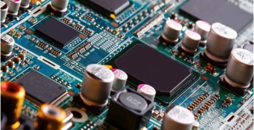
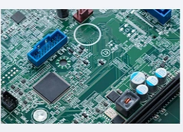
Take the high-definition picture first when you get the circuit board, take both sides, multi-angle, no dead ends. Clear pictures are of great help to the future work, especially when there is only one board.
Second step
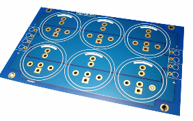
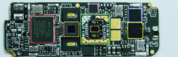
Pick off the materials on the PCB board, first pick the perishable components. The principle of high first, bottom second, there is a re-photograph of small chip components under high components. Take off the device and make a mark. Remember to pick messy and missed picks. If you don't have a tag, you should add it yourself, so that the PCB board and the material are consistent. After removing the device, clean the PCB light board to make it clean and flat.
third step
Find out the corresponding specifications and models for the marked materials one by one. Measure the size and prepare the BOM file.
the fourth step

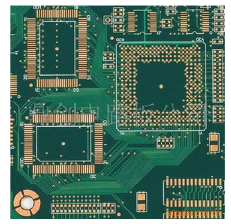
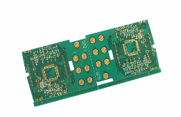
Scan the picture of the PCB board from which the materials have been picked up with a scanner, both sides are required. Scan out pictures with higher resolution as much as possible. Use Photoshop to adjust the picture to a suitable size and sharpness. Our engineers will use Protel 99 and quickpcb software or CAD. This depends on personal preferences and file needs. Draw PCB1:1 traces, copper blocks, vias, pads, and silk screens one by one. After drawing the top and bottom layers, the double panels will be OK. If it is a multi-layer board, the top layer and the bottom layer should be rubbed off with gauze. This process requires engineers with many years of work experience to do. Because some boards with blind and buried holes are easily worn through and missed. Thus scrapped. Grind one layer, sweep one layer, and draw one layer. In this way, there will be no chaos and no mistakes. Check and compare after painting.
the fifth step
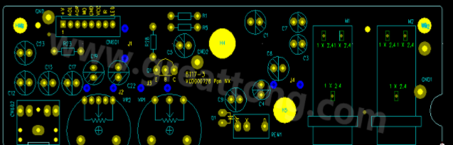
Draw the schematic diagram according to the PCB file and the BOM file, and keep the file.
PCB copy board technology
PCB copy board, currently in the industry is often referred to as circuit board copy board, circuit board clone, circuit board copy, PCB clone, PCB reverse design or PCB reverse research and development. Regarding the definition of PCB copy board clone, the industry and academia have There are many opinions, but they are not complete. If we want to give an accurate definition of PCB copy board cloning, we can learn from the authoritative PCB copy board laboratory in China: PCB copy board, that is, there are already physical objects and circuits of electronic products. Under the premise of the actual board, use reverse R&D technology to reversely analyze the circuit board, and copy the original product's PCB template, materials, schematic files and other technical documents and PCB silk screen production documents 1:1, and then reuse These technical documents and production documents are used for PCB manufacturing, component welding, flying probe testing, circuit board debugging, and complete copying of the original circuit board template. Since electronic products are composed of various types of circuit boards, the core control part performs their work. Therefore, the use of a process of PCB copying can complete the extraction of a full set of technical data of any electronic product, as well as the imitation and cloning of products.
Many people have misunderstood the concept of PCB copy board. In fact, with the continuous development and deepening of the copy board industry, today's PCB copy board concept has been extended to a wider range and is no longer limited to simple circuit board copying and cloning., It will also involve the secondary development of products and the research and development of new products. For example, through the analysis and discussion of existing product technical documents, design ideas, structural features, process technology, etc., it can provide feasibility analysis and competitive reference for the development and design of new products, and assist R&D and design units to follow up the latest in time Technological development trends, timely adjustment and improvement of product design plans, and research and development of the most competitive new products in the market. At the same time, the process of PCB copying can realize the rapid update, upgrade and secondary development of various types of electronic products through the extraction and partial modification of technical data files. The customer's wishes optimize the design and modification of the PCB, reducing some unnecessary circuits. Change some imported devices into domestic ones, after all, some domestically made things are also good. On this basis, it can also add new functions to the product and redesign it, adding its own product logo. In this way, PCB products with new functions will be unveiled at the fastest speed and with a brand new attitude. Not only will they have their own intellectual property rights, they will also win the opportunity in the market and create double benefits.