This is an in-depth article on a very important topic that PCB designers should master. The first thing to remember is that due to discontinuous impedance, signal reflections will occur in the PCB transmission line.
The transmission line should have uniform characteristic impedance. Any change or discontinuity in impedance will cause signal reflection and distortion.
This phenomenon also applies to PCB traces and transmission lines. The reason is that the physical wavelength of the high-frequency signal is very short. Therefore, PCB traces exhibit the same characteristics. The higher the frequency, the shorter the wavelength. You must even treat shorter traces like transmission lines.
Signal trajectory discontinuities or non-uniform discontinuities form signal integrity discontinuities. In order to avoid signal distortion at the source and target, you must match the PCB trace impedance to the source. Then you must load impedances at the source and target ends. This presents a considerable challenge, requiring careful PCB design to mitigate the effects of signal attenuation caused by impedance discontinuities. The greater the discontinuity of the characteristic impedance, the higher the signal reflection. This means that the signal distortion is also higher. Therefore, try to keep the impedance discontinuity as small as possible. In terms of amplitude and time. Read: Why controlled impedance is really important.
Impedance discontinuity affects signal integrity

In theory, the digital signal is a square wave pulse that switches in a short period of time. Naturally, the short signal rise times required by high-frequency digital circuits will result in extremely high frequencies associated with fast signal rise times. In fact, these frequencies will be an order of magnitude higher than the clock frequency of the circuit. The pulse width of high-frequency digital circuits is shorter. Thereby a shorter rise time. A very short signal rise time means that the digital signal contains very high frequencies. Therefore, high-frequency digital signals should follow the signal integrity rules related to high-frequency signals.
Therefore, any changes in the impedance of the PCB traces will cause signal reflections. These can cause ringing and signal distortion. The result of this is that at high switching frequencies, the impedance discontinuity causes serious distortion to the digital signal, and signal sampling errors may occur. You can characterize the transmission line formed by PCB traces with the following parameters: resistance, conductance, and trace resistance. Read the difference between microstrip line and stripline in PCB.
Typical impedance discontinuity
The characteristic impedance of the line is the square root of the inductance divided by the capacitance. This is a reasonable assumption for PCBs because the trace resistance and conductance at high signal frequencies are negligible compared to its inductance and capacitance.
Impedance discontinuity is any factor that affects the ratio of trace inductance to its capacitance. Here are some typical examples:
Impedance changes in the line: If the impedance of the line changes for any reason, such as a change in the copper cross-section or a change in the routing path, the mutual inductance will change and impedance discontinuity will occur.
Branches in the line: Although it may be necessary to route the signal to multiple devices, the use of branches and line stubs can change the line impedance and cause discontinuities.
Return signal splitting: High-frequency signals propagate along the path with the lowest impedance, which is located directly under the signal trace, usually in the ground plane. Any physical feature in the return line or ground plane that forces the return signal to deviate from this path will cause discontinuities.
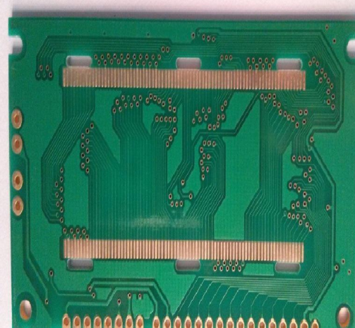
Vias: Use vias to transmit signals from one layer of the PCB to another. Although it is a basic feature of PCB design, the shape and size of the vias will change the inductance and capacitance of the trace, creating another discontinuity. To learn more, read how to reduce parasitic capacitance in PCB layout.
How to limit the impact of impedance discontinuity
The key to controlling the negative effects of impedance discontinuity is to treat all PCB signal traces as transmission lines. You should ensure that the characteristic impedance of all points on the signal path are the same.
Make sure you follow the following guidelines:
Match source impedance and load impedance: Ensure that the source impedance and load impedance are the same as the trace impedance. You can achieve this by using series or parallel resistors to achieve the correct impedance. In addition, you must terminate any open traces with resistors of the correct value.
Avoid branching: If the signal must be shared by multiple chips, connect the lines in a daisy chain instead of using branches. Alternatively, a matching buffer device can be used to transmit the signal to the branch.
Signal return path: Ensure that the signal return follows the same path as the signal line. If using a ground plane, make sure that there is no interruption to the splitting of the return signal path. Make sure that there is a solid plane that runs through the entire length under the trace, and there are no cracks or cuts. If there is no solid plane, use a thicker return trace, which should cover three times the length of the trace and the height of the dielectric.
Via design: Arrange high-frequency traces on a layer as far as possible. If vias are required, please use micro vias instead of traditional vias. Since through holes have significantly different capacitance and inductance characteristics, minimize their use on signal traces. Where necessary, use micro vias with much smaller capacitance and inductance than standard vias. The micro-holes also help keep the stub length as short as possible. Another method is to use high-density interconnection or HDI PCB technology.
Impedance discontinuity and signal reflection
The signal on a uniform transmission line will encounter a constant impedance "Zc (V/I)" at all positions on the line, and the signal will be transmitted along it as needed. However, if there is an impedance discontinuity at any point, signal propagation will be affected, and signal reflection will occur, just as light will reflect when it encounters a discontinuity in the medium in which it propagates.
Various types of impedance discontinuities and their possible causes:
Since the impedance of the transmission line depends on the geometry of the conductor and the characteristics of the PCB material, any change in these characteristics will cause the impedance to change. Some examples are listed here:
At the source or destination/end of the line. The source impedance or receiver impedance is usually different from the impedance of the line.
The change in the line width or height (ie copper thickness) of the PCB material between the signal line and the return path or the change in height and/or dielectric constant.