Designing custom PCB layouts for your complex electronic projects often presents challenges. A simple mistake, no matter how small it looks, can cause your project to malfunction. These common mistakes in PCB design from the beginning can also increase the manufacturing cost of custom PCBs.
This article will explain 15 common mistakes you should know and avoid when designing a custom PCB. Don't worry, even if you are a novice, even an experienced engineer will make these mistakes. Avoiding them will mean high-quality products, lower production costs for custom PCBs, no manufacturing delays, and no rework requirements. So let's get started.
Regardless of available PCB design tools
Designers usually do not consider all available and easy-to-use custom PCB design tools. This is a serious mistake, because there are many design tools that can meet the various needs and flexibility requirements of PCBs. You can use custom PCB design software to perform tasks such as scanning for design errors, component placement, and prototyping. The software is very cheap, web-based, and can even be accessed for free.
Narrow high current trace
If your project must handle currents that are more important than a few hundred milliamps, then narrow PCB trace widths are not enough. Remember that with the same thickness, the outer PCB traces can carry higher currents than the inner layers. The reason is that the former has more heat dissipation and airflow.

Many custom PCB manufacturers will provide you with copper weight options ranging from 0.5 ounces/square foot to 2.5 ounces/square foot. We recommend that you use the trace width calculator to calculate its current carrying capacity.
Improper placement of decoupling capacitors
Decoupling capacitors in custom PCB designs provide services for pins that require stable and clean voltage. You can place them close to the pins to get enough, calm energy. In addition, the power traces of the power rail are also connected to the bolts through decoupling capacitors. You can also make a low-pass filter with an inductor in series to eliminate any input noise.
No optimized switching regulator layout
In electronic custom PCB design, there are two types of regulators: linear regulators and switching regulators. Linear regulators are easy to lay out and inexpensive, but they waste a lot of power. However, although switching regulators are complex, they are very efficient because they consume very little energy. With them, you will get longer battery life. Therefore, it is important to follow the data sheet guidelines when doing PCB layout.
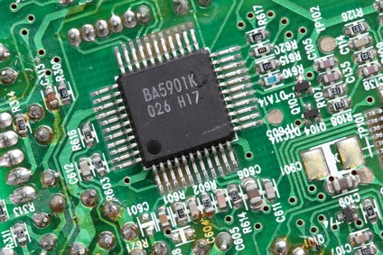
Error when drawing landing mode
The software for custom PCB design provides libraries for components containing PCB landing patterns and schematic symbols. If you only use library components, there will be no problems. But you need to manually draw the landing patterns and schematic symbols of parts that do not yet exist. Therefore, you need to be careful, because even if the pad-to-pad spacing is only one millimeter away, there will be soldering and alignment issues.
Unmanufactured buried or blind holes
If the budget is limited, we recommend that you do not use blind or buried vias in PCB prototyping. Through holes pass through all layers of the PCB, they will definitely increase the size of the PCB. However, they are cheaper than buried or blind vias. The embedded system is electrically connected to the two inner layers, and the blind hole connects the inner layer and the outer layer.
It is worth mentioning that this is not as easy as it sounds. When designing a custom PCB layout, you need to maintain design constraints related to layer stacking.
Improper antenna layout
The antenna custom PCB layout is very important for electronic projects using wireless technology. Even electrical engineers sometimes draw it incorrectly. You may need to match the complex impedance of the antenna and transceiver to achieve maximum power transfer. Therefore, for this purpose, a suitable transmission line is required.
For most antennas, a transmission line with 50 ohm impedance is sufficient to transmit the maximum power. You can use a free online calculator (such as AppCAD) to find out the ratio of the transmission line. You can also place an LC pi network between the transceiver and the antenna to fine-tune the antenna impedance.
Long high-speed routing
High-speed signals should use the straightest and shortest available path. This will help if you point at any high-frequency crystals while properly designing the custom PCB. Many microcontroller-based PCB designs require only a few high-speed signals. Nevertheless, if your project has a high-speed microprocessor, address bus, and external data, then you need to be vigilant.
Did not get a second opinion
Engineers usually work within tight deadlines and focus on obtaining the results of custom PCB production. Causes custom PCB design errors. Therefore, it is best to have another engineer review your PCB design to avoid the high cost of custom PCB production. The rule is simple: if you find errors later, the errors will become more expensive.
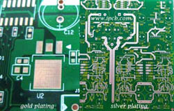
Large skater
Talc is a piece of copper that remains undissolved during chemical etching. It seems that these are attached to the PCB and customized PCB manufacturing appearance, which can also cause short circuits. Therefore, it will help if you ensure that the minimum copper width is greater than the custom PCB manufacturer's requirements. In this way, the coasting will be reduced and your PCB will work normally.
Complex custom PCB design
If a custom PCB manufacturer understands its basic working principle, it can produce PCBs more efficiently and economically. However, if the design is complex, problems such as unbalanced schematics may arise. Therefore, you must try to simplify your custom PCB design to avoid any design errors. In addition, this will increase the effectiveness of your design.
Using incorrect components or custom PCB layout methods
The hour’s need is to use smaller components and a smaller footprint to design complex custom PCB layouts. To this end, designers use ball grid array packaging and embedded devices on the inner layer of the PCB. It helps improve project performance and allows rework in the event of any errors.
You must choose the correct layout method for components with smaller pitches and higher pin counts. Doing so during the design phase will save your custom PCB production costs. In addition, if you plan to use a replacement component, be sure to check whether its performance characteristics match the original component, so as not to discard the customized PCB design at a later stage.
Custom PCB layout-forget to save all PCB design files
Always back up your custom PCB design files. If your software does not respond at first, the files may be lost, so don't wait until the entire design is complete before saving them. You should at least store files that are difficult to retrieve. Most custom PCB manufacturers provide daily backups, but smaller companies may not provide such facilities. In addition, if you work alone at home, this will not be possible.
With the emergence of "cloud" services today, there is no reason to safely backup PCB design files. If you plan to mass-produce your product or want to put it on the market, this will also ensure that your custom PCB design is protected from fire, counterfeiting, threats, malware, and other technological disasters.
Don't consult custom PCB manufacturers early
Custom PCB manufacturers usually follow their registered production processes to improve the efficiency of their employees and equipment. If you do not pay attention to their manufacturing methods, your project costs may rise or manufacturing delays. You will also waste time because you need to contact another custom PCB manufacturer. In addition, you may need to redesign the custom PCB layout according to the manufacturer's specifications.
Custom PCB layout-no need to test custom PCB
Once you have made a customized PCB prototype, you should check it thoroughly. It should be ensured that the initial operating requirements of the design are met. In addition, you can also test environmental conditions that may affect the stability or reliability of the PCB. That is to ensure the extensive operation of your custom PCB. If you don't do this, your custom PCB prototype may fail when it is finally put on the market.