Introduction to the types of pads in the PCB board and application advantages
Circular pads-widely used in single and double-sided printed boards with regularly arranged components. If the density of the board allows, the pad can be larger so that it will not fall off during soldering.
Island-shaped pad-the connection between the pad and the pad is integrated. It is often used in vertical irregular arrangement installation. For example, such pads are often used in tape recorders.
Polygonal pads-used to distinguish pads with close outer diameters but different apertures for easy processing and assembly.
Oval pad-This pad has enough area to enhance the anti-stripping ability, and is often used in dual in-line devices.
Open-shaped pads-in order to ensure that after wave soldering, the pad holes that are manually repaired are not sealed by solder.
Square pads-more used when the printed circuit board components are large and few, and the printed wires are simple. It is easy to use this kind of pads when making the PCB by hand.

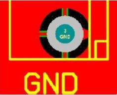
Plum blossom pad
1. The fixing hole needs to be non-metallized. During wave soldering, if the fixing hole is a metalized hole, the tin will block the hole during the reflow soldering process.
2. Fixing mounting holes as quincunx pads is generally used for mounting hole GND network, because generally PCB copper is used to lay copper for GND network. After quincunx holes are installed with PCB shell components, in fact, GND is connected to the earth. On occasion, the PCB shell plays a role of shielding. Of course, some do not need to connect the mounting hole to the GND network.
3. The metal screw hole may be squeezed, resulting in a zero-boundary state of grounding and ungrounding, resulting in a strange abnormality of the system. The plum blossom hole, no matter how the stress changes, can always keep the screw grounded.
Cross pattern pads: Cross pattern pads are also called thermal pads, hot air pads, etc. Its function is to reduce the heat dissipation of the pad during soldering, so as to prevent the virtual soldering or PCB peeling caused by excessive heat dissipation.
Introduction to the types of pads in the PCB board and application advantages
1. When your pad is ground. The cross pattern can reduce the area of the ground wire, slow down the heat dissipation speed, and facilitate welding.
2. When your PCB requires machine placement and is a reflow soldering machine, the cross pattern pad can prevent the PCB from peeling (because more heat is needed to melt the solder paste).
Teardrop pad: A teardrop is an excessive drip connection between a pad and a wire or a wire and a via. The purpose of setting a teardrop is to prevent the wire and the pad or the wire from being impacted by a huge external force. The contact point of the guide hole is disconnected, and the placement of teardrops can also make the PCB circuit board look more beautiful.
1. When soldering, it can protect the pad and avoid the falling off of the pad due to multiple soldering.
2. Strengthen the reliability of the connection (production can avoid uneven etching, cracks caused by via deviation, etc.)
3. Smooth impedance and reduce the sharp jump of impedance
In the circuit board design, in order to make the pad stronger and prevent the pad and the wire from being disconnected during the mechanical manufacturing of the board, a copper film is often used to arrange a transition area between the pad and the wire, which is shaped like a teardrop, so it is often called Fill teardrops.