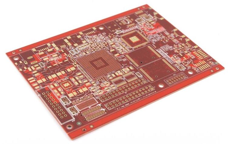
Non nickel PCB surface treatment process of Multilayer PCB, The final PCB surface treatment process for Multilayer PCB manufacturing has undergone important changes in recent years. These changes are the result of the continuous demand to overcome the limitations of HASL (hot air solver level) and more and more HASL alternative methods.
The final PCB surface treatment process is used to protect the surface of circuit copper foil. Copper (Cu) is a good surface of welding elements, but it is easy to oxidize; Copper oxide hinders the wetting of solder. Although gold (AU) is now used to cover copper, because gold does not oxidize; Gold and copper will rapidly diffuse and penetrate each other. Any exposed copper will soon form non weldable copper oxide. One method is to use a "barrier layer" of nickel (Ni), which prevents the transfer of gold and copper and provides a durable and conductive surface for the assembly of components.
Requirements for surface treatment process of non electrolytic nickel PCB for Multilayer PCB

The surface treatment process of non electrolytic nickel PCB should complete several functions:
Gold precipitated surface
The ultimate purpose of the circuit is to form a connection with high physical strength and good electrical characteristics between multilayer PCB circuit boards and components. If there is any oxide or contamination on the surface of Multilayer PCB, this welding connection will not occur with today's weak flux.
Gold naturally precipitates on nickel and will not oxidize in long-term storage. However, gold will not precipitate on oxidized nickel, so nickel must remain pure between nickel bath and gold dissolution. Thus, the first requirement for nickel is to remain free of oxidation for a long enough time to allow the precipitation of gold. The element developed a chemical immersion bath to allow a phosphorus content of 6 ~ 10% in the precipitation of nickel. This phosphorus content in the surface treatment process of non electrolytic nickel PCB is considered as a careful balance of bath control, oxides, and electrical and physical properties.
hardness
Non electrolytic nickel PCB surface treatment process is used in many applications requiring physical strength, such as automobile transmission bearings. The need for Multilayer PCB is far less stringent than these applications, but a certain hardness is still important for wire bonding, touch pad contact points, edge connectors and processing sustainability.
Wire bonding requires a nickel hardness. If the lead deforms the sediment, the loss of friction may occur, which helps the lead "melt" to the substrate. SEM photos showed no penetration into planar nickel / gold or nickel / palladium (PD) / gold surfaces.
Electrical characteristics
Because it is easy to make, copper is selected as the metal formed by circuits. Copper is superior in conductivity to almost every metal. Gold also has good conductivity and is the perfect choice for the outermost metal because electrons tend to flow on the surface of a conductive route ("surface" benefit).
Copper 1.7 µ Ω cm
Gold 2.4 µ Ω cm
Nickel 7.4 µ Ω cm
Non electrolytic nickel coating 55 ~ 90 µ Ω cm
Although the electrical characteristics of most production boards are not affected by the nickel layer, nickel can affect the electrical characteristics of high-frequency signals. The signal loss of Microwave Multilayer PCB can exceed the designer's specification. This phenomenon is proportional to the thickness of nickel - the circuit needs to pass through the nickel to the solder joint. In many applications, the electrical signal can be restored to the design specification by specifying a nickel precipitation of less than 2.5 µ M.
contact resistance
Contact resistance is different from weldability because the nickel / gold surface remains non welded throughout the life of the end product. Nickel / gold must maintain the conductivity of external contact after long-term environmental exposure. Antler's 1970 work quantifies the contact requirements for nickel / gold surfaces. Various end uses were studied.