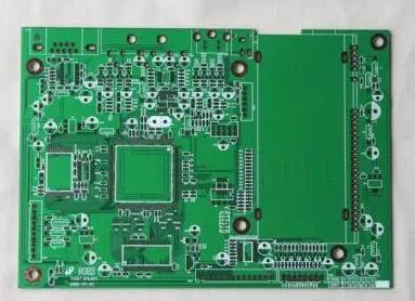
Three Manufacturing Methods of Printed Circuit Boards (PCBs):Substractive,msap,sap
(1) Substractive Process the PCB laminate is covered with a layer of copper foil, the lines that need to be retained are covered with a coating, and the exposed copper foil is removed by etching to form the required lines.
(2) msap (Modified Semi-additive Process) - a very thin copper layer is first formed on the surface of the PCB material, and then the lines that do not need to be retained are covered with a coating, and the required lines are exposed and are added by electroplating. Then,after removing the coating, the thin copper layer that has not been thickened is removed by micro-etching, and finally the required circuit is formed.
(3) SAP (Semi-additive Process) - by means of photocopying/printing/laser activation,a preliminary copper circuit is directly formed on the plate, and then thickened by electroplating or electroless plating to form the required circuit.

Three PCB Manufacturing Methods
With the emergence of new mSAP (Modified Semi-additive Process) technology on PCB, its trace width can be reduced by half to reach the level of 1.25mils, so the circuit assembly density can be maximized. At present, the continuous progress of integrated circuits has been transferred from the semiconductor IC lithography process (Lithography) to the PCB process.
At present, the most commonly used subtractive PCB process in the industry, its wiring width tolerance tolerance can reach a minimum of 0.5mil. The test results of iPCB show that if the wiring width exceeds 3 mils and the signal edge rate is relatively low, although the change value of 0.5 mil is not obvious, it has a significant impact on the impedance control of thinner wiring.
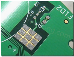
The PCB process basically covers one or both sides with a copper-containing substrate material, that is, Core. The material and thickness of copper substrates used on the substrates produced by each PCB manufacturer are different, so the insulation and mechanical properties are also different.
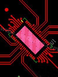
Next, the copper foil and the substrate material are pressed together to form a substrate, and then the substrate is covered with an anti-corrosion agent and then exposed, and then the unexposed anti-corrosion agent and copper are etched in an acid bath to form wiring. The purpose of this method is to make the wiring form a rectangular section, but during the acid tank process, not only will the copper on the vertical plane be eroded, but also part of the wiring wall on the horizontal plane will be dissolved.
Under the strict control of the subtractive PCB process, the wiring can form a trapezoidal cross-section of almost 25~45 degrees. However, if it is not properly controlled, the upper half of the wiring will be over-etched, resulting in the result that the upper part is narrow and the lower part is thick. The etch factor is obtained by comparing the height of the etched wiring with the eroded depth of the upper half of the wiring, and the larger the value, the more rectangular the cross-section of the wiring is.

Once the routing can be rectangular, the Impedance is more predictable, and the repeatable layout can be achieved at almost vertical angles, which means that the circuit assembly density can be maximized, and the PCB manufacturing yield can also be improved from a signal integrity perspective.
The same way to achieve this result is mSAP (Modified Semi-additive Process). In this method, the substrate is laminated with a copper foil with a thinner thickness of 2 or 3 micrometers (μm), and then a via hole is drilled and covered with electroless copper.
Next, an anti-corrosion agent is added in a specific area for exposure to form the desired wiring. After the exposed areas are stacked, the remaining copper is allowed to etch, so this method is basically the opposite of the subtractive method. Compared with the chemical principle of the subtractive method, part of the mSAP wiring basically uses Photolithography. Therefore, the width of the wiring formed by the latter is more in line with the original design.
Under extremely tight tolerances, the trace width can maintain a level of 1.25mils with a certain level of impedance control. The actual measurement found that the impedance change measured by the entire PCB board will not exceed 0.5ohm, which is 1/5 of the subtraction method.
The test results of iPCB show that precise impedance control is indispensable to meet the requirements of high-speed digital systems and microwave applications, which can also be achieved through mSAP. Moreover, it can achieve almost vertical wiring design characteristics, and can also maximize the circuit assembly density.