Language
Get quotes quickly.
sales@ipcb.com
2021-11-23
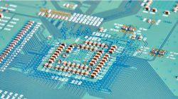
Microwave PCB dielectric ceramics refers to a new type of ceramic functional material used in microwave frequency circuits (mainly in the 300MHz ~ 300GHZ frequency band).
2021-11-22
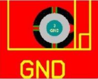
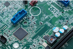
Introduction to the types of pads in the PCB board and application advantagesCircular pads-widely used in single and dou...
Performance and Characterization of OSP Film in the Lead-Free Process of PCB Copy BoardThe OSP film is mainly composed o...
2021-11-19
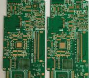
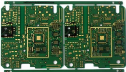
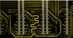
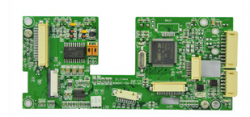
HDI board that is high-density interconnection board, is a circuit board with a relatively high line distribution densit...
2021-11-18
First,What is fiberglass PCB boardThe alias of glass fiber board: glass fiber heat insulation board, glass fiber board (...
2021-11-12
So, are you all ready to design your first PCB prototype? We believe this must be a surprise moment for you. We thank yo...
Since 2016, the PCB industry has recovered as a whole, and the supply-demand relationship of the industry chain has unde...
What are the experiences of PCB manufacturing in China
The full name of AOI (Automatic Optic Inspection) is automatic optical inspection, which is based on optical principles ...
When it comes to printed circuit boards, many people and companies consider important aspects such as quality, functiona...
In recent years, affected by the economic situation, the global printed circuit board (PCB) market has maintained steady...
Designing custom PCB layouts for your complex electronic projects often presents challenges. A simple mistake, no matter...
The general trend of eastward shifting of industries has led the mainland to thrive. The focus of the PCB industry is co...
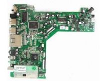
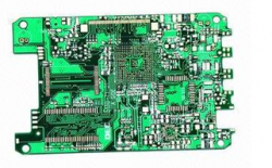
PCB (Printed Circuit Board) is mainly divided into rigid board, flexible board, IC package substrate and so on. Essence ...
At present, a series of active domestic policies to encourage the development of the PCB industry have guided the PCB in...
A pattern is a repetitive sequence of repeated designs, mainly decorative. All printed circuit boards have patterns, and...
Apple is optimistic about the prospects of liquid crystal polymer resin materials. It rarely spends huge sums of money o...
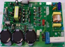
Industrial PCB manufacturing process:Industrial PCB design:When it comes to industrial PCB manufacturing, PCB design and...
I feel that under the development of global science and technology, the earth's resources are facing a crisis of gra...
Industrial PCB materials:The selection of PCB materials is a very important step in PCB manufacturing.This is because th...