p>General'in temel tasarım süreci
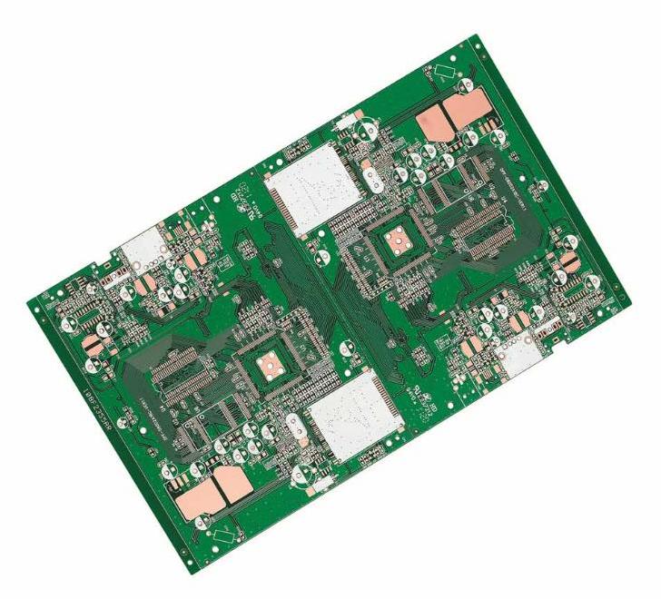
PCB tahtası is as follows
1. Preliminary preparation
This includes preparing component libraries and schematics. "Eğer iyi bir iş yapmak istiyorsan, İlk önce aletlerinizi kesmelisiniz.İyi bir tahta yapmak için, prensipleri tasarlamak için, Siz de iyi çizmelisiniz.. Şunu tasarlamadan önce PCB tahtası, SCH'nin şematik diagram ının komponent kütüphanesini ve komponent kütüphanesini hazırlayın. PCB tahtası. Komponent kütüphanesi protel ile gelen kütüphaneyi kullanabilir., ama genelde uygun bir tane bulmak zordur.. Seçilen aygıtların standart boyutlu verilerine göre kendinize bir komponent kütüphanesi oluşturmak daha iyi.. Principle., Bölge kütüphanesini PCB tahtası ilk, ve sonra SCH'nin komponent kütüphanesini. Kütüphane PCB tahtası yüksek ihtiyaçları var., kurulun kurulmasını doğrudan etkileyici; SCH'nin komponent kütüphane ihtiyaçları oldukça açık, Pin özelliklerini ve ilişkileri tanımlamak için dikkatini çektiğiniz sürece PCB tahtası komponentler. PS: Standart kütüphanedeki gizli piyonları notla. Bundan sonra şematik diagram ının tasarımı, ve sonrasında, başlamak için hazır. PCB tahtası tasarlama.
2. PCB tahtası structure tasarlama
In this step, kararlı devre tahtası boyutuna ve çeşitli mekanik pozisyonuna göre, çiz PCB tahtası yüzeyi PCB tahtası tasarlama ortamı, ve gerekli bağlantıları, buttons/değiştirmeler, Döşekleri fırlat., toplama delikleri, etc.. pozisyon gerekçelerine göre. And fully consider and determine the wiring area and non-wiring area (such as how much area around the screw hole belongs to the non-wiring area).
3. PCB tahtası layout
The layout put it bluntly is to put the device on the board. Şu an, yukarıdaki hazırlıklar, you can generate a netlist (Design-Create Netlist) on the schematic diagram, and then import the netlist (Design-Load Nets) on the PCB tahtası diagram. Aygıtlar toplandığını gördüm., and there were flying wires between the pins to indicate the connection. The device can then be placed. The general layout is carried out according to the following principles:
1) According to the reasonable division of electrical performance, it is generally divided into: digital circuit area (Bu,, afraid of interference and interference), analog circuit area (afraid of interference), and power drive area (interference source);
2) The circuit that completes the same function should be placed as close as possible, ve komponentler bağlantının basit olmasını sağlamak için ayarlanmalıdır; aynı zamanda, the relative position of each functional block should be adjusted to make the connection between the functional blocks simple;
3) For components with large mass, yerleştirme pozisyonu ve yerleştirme gücünü düşünmeli; ısıtma elementleri sıcaklık hassas komponentlerden ayrı yerleştirilmeli, and thermal convection measures should be considered if necessary;
4) The I/O drive device should be as close as possible to the edge of the printed board and the lead-out connector;
5) The clock generator (such as crystal oscillator or clock oscillator) should be as close as possible to the device that uses the clock;
6) A decoupling capacitor (usually a monolithic capacitor with good high-frequency performance) needs to be added between the power input pin of each integrated circuit and the ground; when the circuit board space is dense, Ayrıca birkaç integral devre etrafında yerleştirilebilir.
7) A discharge diode should be added to the relay coil (1N4148);
8) The layout requirements should be balanced, yoğun ve düzenli, and should not be top-heavy or heavy. Komponentleri yerleştirildiğinde, the actual size of the components (occupied area and height) and the relative position between components must be considered. To ensure the electrical performance of the circuit board and the feasibility and convenience of production and installation, the placement of the devices should be appropriately modified on the premise that the above principles can be reflected to make them neat and beautiful. Örneğin, aynı aygıtları düzgün ve yönlendirmelidir. Doğru, "patched" değil.. Bu adım tahta'nın bütün görüntüsüyle ve sonraki adımda sürüşme zorluğuyla bağlantılı., bu yüzden düşünmek için çok çalışma gerekiyor.. Geçtiğinde, emin olmayan yerler için ilk yönetim yapabilirsiniz, ve onları tamamen düşünüyoruz..
4. Wiring
Wiring is an important process in the entire PCB tahtası tasarlama. Bu, direkt etkileyecek PCB tahtası. Düzenleme sürecinde PCB tahtası, Genelde üç bölüm var: ilk bölüm, bunun için PCB tahtası design. Eğer çizgiler açılmazsa, and there are flying wires everywhere, Bu, bilinmeyen bir tahta olacak., ve henüz başlamadığını söyleyebilir.. İkincisi elektrik performansının memnuniyeti.. Bu, basılı devre tahtasının. Bu yoldan sonra, en iyi elektrik performansını elde edebilmek için. Sonraki güzellik.. Eğer sürücünüz bağlanıyorsa, elektrik makinelerin performansını etkileyecek hiçbir şey yok, ama ilk bakışta, Berbat görünüyor., colorful and colorful, elektrik performansınız ne kadar iyi olursa olsun, Hala başkalarının gözlerinde bir çöp parçası.. Bu testi ve tutuklama için büyük rahatsızlık getirir.. Dönüş temiz ve üniforma olmalı., hiçbir kural olmadan. Bunların hepsi elektrik aletin performansını ve diğer özel ihtiyaçlarını yerine getirmek ve başka özel ihtiyaçlarını sağlamak için gerçekleşmelidir., yoksa terk edilecek. The wiring is mainly carried out according to the following principles:
1) In general, elektrik hattı ve yerel hattı ilk olarak devre tahtasının elektrik performansını sağlamak için. İzin verildiği kadar, güç ve yerel kabloların genişliğini genişletip, tercih ederse yeryüzü kablosu güç kablosundan daha geniş, and their relationship is: ground wire > power wire > signal wire, genellikle sinyal kablo genişliği:0.2- 0.3mm, Zayıf genişlik 0'a ulaşabilir..05- 0.07mm, ve güç kablosu genelde 1.2- 2.5 mm. Şimdi... PCB tahtası sayısal devre, geniş bir yer kablosu bir döngü oluşturmak için kullanılabilir, that is, a ground network can be used (the ground of the analog circuit cannot be used in this way).
2) Wire the lines with strict requirements (such as high-frequency lines) in advance, ve girdi sonu ve çıkış sonu arasındaki yakın paralel çizgilerden uzak durun, yansıtma aracılığından uzak durun.. Eğer gerekirse, Yer kablo izolasyonu eklemeliyiz., ve iki yakın katın dönüşü birbirine perpendikli olmalı., Parazitik bağlantı kolayca paralel olarak.
3) The oscillator shell is grounded, saat hattı mümkün olduğunca kısa olmalı., ve her yerde çizim olmamalı.. Saat oscilasyon devrelerinin altında, özel hızlı mantıklı devre parçası yeryüzünün bölgesini arttırmalı., and other signal lines should not be used to make the surrounding electric field approach zero;
4) Use 45-degree folded lines as much as possible, and do not use 90-degree folded lines to reduce the radiation of high-frequency signals; (double arcs should also be used for lines with high requirements)
5) Do not form a loop in any signal line. If it is unavoidable, the loop should be as small as possible; the vias of the signal line should be as few as possible;
6) The key lines should be as short and thick as possible, ve korumalı yer iki tarafta eklenmeli.
7) When transmitting sensitive signals and noise field signals through flat cables, "Yer kablo-sinyal-zemin kablosunu kullanın".
8) Test points should be reserved for key signals to facilitate production and maintenance testing
9) After the schematic wiring is completed, yönlendirme iyileştirilmeli; aynı zamanda, after the preliminary network inspection and DRC inspection are correct, boşaltma bölgesi yeryüzü kablolardan doludur., ve toprak kabloları için büyük bir bakra katı kullanılır.. Kullanılmayan yerler yere bağlı bir kablo olarak bağlanıyor.. Ya da çoklu katı yap.
PCB tahtası, enerji temsili, Yer kablosu her bir katı alır.