電路板打樣生產工藝介紹
的創建者 印刷電路板 is the Austrian Paul Eisler (Paul Eisler), 1936年, 他首先使用 印刷電路板 在收音機裏. 1943年, 美國人大多將這項科技用於軍用無線電. 1948年, 美國正式批准這項發明用於商業用途. 自2.0世紀50年代中期以來, 印刷電路板s才剛剛開始被廣泛使用.
在PCB板出現之前, 電子元件之間的互連是通過電線直接完成的. 現今, 電線僅在實驗室中用於測試應用; 印刷電路板打樣 has definitely occupied an absolute control position in the electronics industry.
PCB production process:
1. Contact the manufacturer
First, 你需要找到 電路板製造商 在Internet上, 然後瞭解公司規模, 產品優勢, 電路板廠地址, and then communicate (QQ or call). 會有相關人員給你報價, 下訂單, 和後續行動. 生產計畫表, 運輸, 傳送.

2. Cutting
Purpose: According to the requirements of the engineering data MI, 在符合要求的大板上, 切割成小塊以製作面板. 滿足客戶要求的小型板材.
工藝:根據MI要求大板材切割板- curium板- beer fillet\grinding - board out
Three, drilling
Purpose: According to the engineering data, 在滿足所需尺寸的板材上的相應位置鑽取所需的孔徑.
Process: stacked board pin - upper board - drilling - lower board - inspection\repair
Fourth, sink copper
Purpose: Immersion copper is to deposit a thin layer of copper on the insulating hole wall by chemical method.
Process: rough grinding - hanging board - automatic copper sinking line - lower board - dip% dilute H2SO4 - thickened copper
Five, graphics transfer
Purpose: Graphic transfer is to transfer the image on the production film to the board
Process: (blue oil process): grinding plate - printing the first side - drying - printing the second side - drying - exploding - developing shadow - inspection; (dry film process): hemp board - pressing film - standing - right Position-Exposure-Standing-Development-Check
Six, graphic plating
Purpose: Pattern electroplating is to electroplate a copper layer with the required thickness and a gold-nickel or tin layer with the required thickness on the bare copper skin or hole wall of the circuit pattern.
Process: upper board - degreasing - second washing with water - micro-等hing - washing - pickling - copper plating - washing - pickling - tin plating - washing - lower board
Seven, remove the film
Purpose: Use NaOH solution to remove the anti-plating coating film to expose the non-circuit copper layer.
Process: water film: insert rack - soak alkali - rinse - scrub - pass machine; dry film: release board - pass machine
Eight, etching
Purpose: Etching is to use a chemical reaction method to corrode the copper layer of non-circuit parts.
九, green oil
Purpose: Green oil is to transfer the graphic of the green oil film to the board to protect the circuit and prevent the tin on the circuit when welding parts.
Process: grinding plate-printing photosensitive green oil-curium plate-exposure-exposure; grinding plate-printing the first side-drying plate-printing the second side-drying plate
Ten, characters
Purpose: Characters are provided as a mark for easy identification
Process: After the green oil finishes - cool and stand - adjust the screen - print characters - rear curium
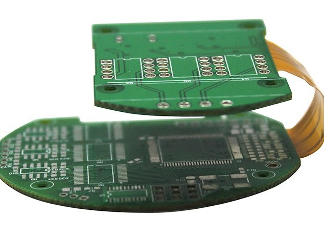
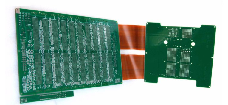
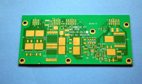
Eleven, gold-plated fingers
Purpose: to plate a layer of nickel/gold with the required thickness on the finger of the plug to make it more hard and wear-resistant
Process: upper plate - degreasing - washing twice - micro-etching - washing twice - pickling - copper plating - washing - nickel plating - washing - gold plating
Tin plate (a process in parallel)
Purpose: Tin spraying is to spray a layer of lead tin on the exposed copper surface that is not covered with solder mask to protect the copper surface from corrosion and oxidation to ensure good soldering performance.
Process: micro-erosion - air drying - preheating - rosin coating - solder coating - hot air leveling - air cooling - washing and air drying
12. Forming
Purpose: through die stamping or CNC gong machine gong forming the shape required by the customer. 有機鑼, 啤酒委員會, 手鑼, hand cutting
Note: The accuracy of the data gong machine board and the beer board is higher. 手鑼是第二個, 而最小的手工砧板只能做出一些簡單的形狀.
13. Test
Purpose: To pass electronic 100% testing to detect defects that affect functionality such as open circuits and short circuits that are not easy to find visually.
Process: upper mold - release board - test - pass - FQC visual inspection - unqualified - repair - return test - OK - REJ - scrap
14. Final inspection
Purpose: To pass 100% visual inspection of board appearance defects, 並修復小缺陷,避免問題和缺陷板流出.
具體工作流程:來料-查看資訊-目視檢查-合格-FQA抽檢-合格-包裝-不合格-加工-檢驗合格
15、真空包裝
16、裝運
iPCB是一家專注於開發和生產高精度PCB的高科技製造企業. iPCB很高興成為您的業務合作夥伴. 我們的業務目標是成為世界上最專業的PCB原型製造商. 主要專注於微波高頻PCB, 高頻混合壓力, 超高多層集成電路測試, from 1+ to 6+ HDI, Anylayer HDI, IC基板, IC測試板, 剛柔PCB, 普通多層FR4 PCB, etc. 產品廣泛應用於工業4.0, 通信, 工業控制, 數位的, 權力, 電腦, 汽車, 醫學的, 航空航太, 儀器儀錶, 物聯網及其他領域.