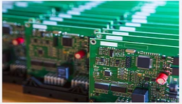
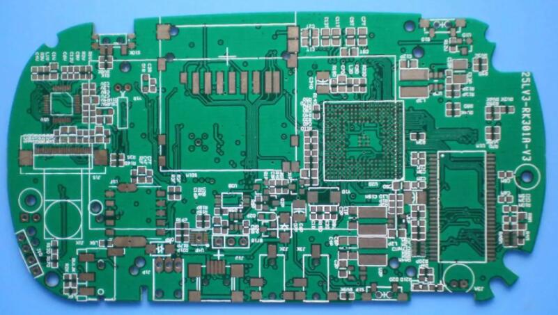
1 pcb design requires a planned design
Although Protel has the function of automatic planning, Он не может полностью удовлетворить требования клиентов высокочастотная плата. It often depends on the designer's experience and according to the detailed situation. Planning to complete the overall design of the PCB circuit board. Whether the planning is reasonable or not directly affects the product's life, устойчивость, EMC (electromagnetic compatibility), сорт., it is necessary to start from the overall planning of the circuit board, совместимость проводов и PCB, mechanical structure, теплоотдача, EMI (electromagnetic compatibility), сорт. Comprehensive consideration in terms of interference), reliability, целостность сигнала.
В общем, Во - первых, поместить узлы в определённое положение, связанное с механическим размером, then place the special and larger components, and finally place the small components. одновременно, необходимо согласовать требования к монтажу, the placement of high-frequency components should be as compact as possible, соединение сигнальных линий должно быть как можно короче, so as to reduce the interference of signal lines.
1.1 The placement of the positioning plug-in related to the mechanical size
Power sockets, switches, interfaces between PCBs, indicator lights, сорт. все модули позиционирования связаны с механическими размерами. В общем, the interface between the power supply and the PCB is placed at the edge of the PCB, and there should be a distance of 3 mm to 5 мм from the edge of the PCB; indicating that the light-emitting diodes should be placed accurately according to the needs; switches and some fine-tuning components, such as adjustable Inductance, adjustable resistance, etc. should be placed close to the edge of the PCB to facilitate adjustment and connection; components that require frequent changes must be placed in a relatively small location for easy replacement.
1.2 Placement of special components
High-power tubes, transformers, rectifier tubes and other heating devices generate more heat when working in high-frequency conditions, so you should think about ventilation and heat dissipation when planning, и поместить эти элементы на PCB, чтобы облегчить циркуляцию воздуха. . The high-power rectifier tube and adjustment tube should be equipped with a radiator and kept away from the transformer. Heat-sensitive components such as electrolytic capacitors should also be kept away from heating devices, Иначе электролит засохнет., resulting in increased resistance and poor performance, это влияет на устойчивость цепи.
Components that are prone to failure, such as adjustment tubes, electrolytic capacitors, эстафета, etc., should be considered for easy maintenance when placing them. контрольно - измерительная точка, care should be taken to ensure that the test rods can be easily accessed when arranging components.
магнитное поле рассеяния 50 Гц, when it is cross-connected with some parts of the low-frequency amplifier, it will interfere with the low-frequency amplifier. поэтому, it is necessary to separate them or stop shielding treatment. It is best to arrange all levels of the amplifier in a straight line according to the schematic diagram. The advantage of this arrangement is that the ground current of each level is closed and active at this level and does not affect the work of other circuits. The input stage and output stage should be as far away as possible to reduce the parasitic coupling interference between them.
рассмотреть связь передачи сигналов между функциональными схемами элементов, the low-frequency circuit and the high-frequency circuit should be separated, and the analog circuit and the digital circuit should be separated. The integrated circuit should be placed in the center of the PCB so that each pin can be connected to the wiring of other devices.
Devices such as inductors and transformers have magnetic coupling and should be placed orthogonally to each other to reduce magnetic coupling. Кроме того, they all have a strong magnetic field, and there should be an appropriately large space or magnetic shielding around them to reduce the impact on other circuits.
Appropriate high-frequency decoupling capacitors should be configured on the key parts of the PCB. например, an electrolytic capacitor of 10 μF ~ 100 μF should be connected to the input end of the PCB power supply, и керамика около 0.01 pF should be connected to the power supply pin of the integrated circuit. Chip capacitors. Some circuits must be equipped with appropriate high-frequency or low-frequency chokes to reduce the influence between the upper and lower frequency circuits. при проектировании и составлении схем следует учитывать это, otherwise it will also affect the performance of the circuit.
The spacing between the components should be appropriate, and the spacing should be considered whether there is a possibility of breakdown or ignition between them.
усилитель, используемый для включения двухтактных и мостовых схем, attention should be paid to the symmetry of the electrical parameters of the components and the symmetry of the structure, so that the dispersion parameters of the symmetrical components are as different as possible.
ручное планирование основного узла после завершения, the method of component locking should be adopted so that these components will not move during the automatic planning. То есть, execute the Edit change command or select Locked in the Properties of the component to lock it and no longer move it.
1.3 Placement of common components
Regarding common components, сопротивление типа, capacitors, etc., Вы должны рассмотреть конфигурацию компонентов, the size of the occupied space, эксплуатационная возможность монтажа, удобство сварки. Automatic planning can be used.

2 Wiring design
Wiring is the overall request for high-frequency PCB design to be completed on the basis of reasonable planning. Wiring includes automatic wiring and manual wiring. Generally, regardless of the number of key signal lines, Сначала остановить ручное соединение этих сигнальных линий. After the wiring is completed, прекратить тщательную проверку этих сигнальных линий. After the inspection, починить, and then stop the automatic wiring of other wiring. То есть, the manual and automatic wiring are separated to complete the wiring of the PCB.
в процессе высокочастотной проводки PCB особое внимание следует уделять следующим аспектам.
2.1 The trend of wiring
The wiring of the circuit is best to use a full straight line in accordance with the flow of the signal, and it can be completed with a 45° broken line or arc curve when changing the machine, Это может уменьшить внешнюю эмиссию высокочастотных сигналов и взаимную связь. The wiring of high-frequency signal lines should be as short as possible. рабочая частота по цепи, the length of the signal line wiring should be selected reasonably, Это может уменьшить параметры расширения частоты, уменьшить потери сигнала. When manufacturing a double-sided board, соединение с двумя соседними слоями желательно вертикально, oblique or curved to intersect each other. предотвращать параллелизм, so as to reduce mutual interference and parasitic coupling.
линия высокочастотных сигналов и низкочастотная сигнальная линия должны быть максимально отделены друг от друга, and shielding measures should be taken if necessary to avoid mutual interference. относительно использования относительно слабых входных зажимов, it is susceptible to interference from external signals. заземляющая линия может быть использована в качестве щита, чтобы окружить ее или экранировать высокочастотное соединение. Следует предотвращать параллельное соединение на одном уровне, otherwise it will introduce scattered parameters and affect the circuit. если не удалось остановить, a grounded copper foil can be introduced between the two parallel wires to form an isolated wire.
в цифровых схемах, the differential signal lines should be routed in pairs, максимально сблизить их, and the length is not much different.
2.2 Wiring method
In the PCB wiring process, минимальная ширина линии следов определяется прочностью связи между проводом и изоляционной плитой, а также токовой прочностью протекающего провода. когда толщина медной фольги равна 0.05 мм and the width is 1mm to 1.5mm, Он может пропускать ток 2А. The temperature will not be higher than 3 . Кроме особых следов, the width of other traces on the same level should be as different as possible. расстояние между проводами в высокочастотных схемах влияет на размер рассеянной емкости и индуктивности, потеря сигнала, circuit stability, помехи от сигнала. In high-speed switching circuits, расстояние между проводами повлияет на время передачи сигнала и качество формы. поэтому, the minimum spacing of wiring should be greater than or equal to 0.5 mm, as long as it is allowed, лучше всего использовать относительно широкую линию для прокладки PCB.
There should be a certain distance between the printed wire and the edge of the PCB (not less than the thickness of the board), это удобно не только для монтажа, но и для остановки механической обработки., but also improves the insulation performance.
когда соединение может быть соединено только с большим кольцом, flying wires should be used, То есть, short wires should be used directly to reduce the interference caused by long-distance wiring.
цепь с магнитными чувствительными элементами более чутко реагирует на окружающее магнитное поле, and when high-frequency circuits work, угол провода может излучать электромагнитные волны. If magneto-sensitive components are placed in the PCB, проследить за тем, чтобы угол провода был отделен от них.
The wiring on the same level is not allowed to be interspersed. линия о возможном рассеянии, Вы можете использовать метод "сверления" и "наматывания", То есть, Пускай проводник "бурится" через зазор под пяткой другого оборудования (например, резистора), capacitors, & триод, or from a line that may be interspersed. ведущий конец "Обход". In special circumstances, Если схема очень сложна, in order to simplify the design, Разрешить также использование межсоединений для решения проблем сквозного пробоя.
Когда рабочие частоты в высокочастотных схемах выше, Необходимо также учитывать совпадение сопротивлений проводов и антенный эффект.
2.3 Wiring requirements for power cord and ground wire
According to the size of different working currents, максимально увеличить ширину линии электропитания. The high-frequency PCB should try to use a large area ground wire and plan it on the edge of the PCB to reduce the interference of external signals on the circuit; at the same time, заземление PCB может быть хорошо контактировано с оболочкой, Таким образом, напряжение заземления PCB ближе к напряжение заземления. The central connection should be selected according to the detailed conditions. это отличается от низкочастотной схемы. The grounding wire of the high-frequency circuit should be grounded nearby or multi-point grounding. заземляющий провод должен быть коротким и грубым, чтобы снизить сопротивление заземления до минимума. The allowable current request can be Reach the specification of 3 times the working current. заземление громкоговорителя должно быть соединено с позицией выходного каскада усилителя PCB. не заземляй его.
в процессе монтажа, some reasonable wiring should be locked in time to avoid repeated wiring. То есть, execute the EditselectNet command and select Locked in the properties of the pre-wiring to lock it and no longer move it.
3 pcb pad and copper design
3.1 Land and aperture
Under the condition of ensuring that the minimum wiring spacing does not violate the designed electrical spacing, прокладка должна быть больше, чтобы обеспечить достаточную ширину кольца. The inner hole of the ordinary pad is slightly larger than the lead diameter of the component, и дизайн большой, и при сварке легко образуется виртуальный припой. The outer diameter D of the pad is generally not less than (d+1.2)mm, где d внутренний диаметр прокладки. Относительно высокая плотность PCB, the minimum value of the pad can be (d+1.0) mm. The shape of the pad is usually set to be circular, Но диск с встроенной интегральной схемой предпочтительнее, чем форма взлётно - посадочной полосы, so that the area of the pad can be increased in a limited space, сварка в пользу интегральной схемы. The connection between the wiring and the pad should be smoothly transitioned, that is, when the width of the wiring into the round pad is smaller than the diameter of the round pad, the teardrop design should be adopted.
Следует отметить, что размер отверстия d В сварной диске неодинаков, and it should be considered based on the size of the lead diameter of the actual component, окно компонента, device holes, прорезь. The hole spacing of the pads should also be considered based on the device method of the practical components. например, resistors, diodes, tubular capacitors and other components have "vertical" and "horizontal" installation methods. Эти два метода отличаются друг от друга. In addition, the design of the pad hole distance must also consider the minimum gap requirements between components, especially the gap requirements between special components are guaranteed by the hole distance between the pads.
In high-frequency PCBs, Следует также свести к минимуму количество отверстий, Это снижает дисперсную емкость и повышает механическую прочность PCB. In short, in the design of high-frequency PCB, the design of the pad and its shape, раскрыв и шаг винта должны учитывать не только их специфичность, but also meet the requirements of the consumer process. The use of standardized design can not only reduce product costs, but also improve the efficiency of consumption while ensuring the quality of production.
3.2 Copper coating
The main purpose of copper coating is to improve the anti-interference ability of the circuit. At the same time, it has great benefits in terms of PCB heat dissipation and PCB strength. покрытие медью и заземление также могут служить экраном. Однако, large-area strip copper foil cannot be used. из - за длительного использования PCB, the strip copper foil is prone to shrinkage and scattered phenomena at this time. Therefore, it is best to use grids when depositing copper. The grid is connected to the grounding network of the circuit, so that the grid will have a better shielding effect. The size of the grid network is determined by the interference frequency to be shielded.
После завершения проектирования монтажа, pads and vias, DRC (Design Rule Check) should be performed. In the inspection results, the differences between the designed diagram and the defined rules are listed in detail, and the network that does not meet the request can be found. However, you should first stop the DRC parameter setting before wiring to run the DRC, that is, Выполнение команды ToolsDesign Rule Check.
4 Conclusion
The высокочастотная платаdesign is a complicated process, and many elements are touched, which may be directly related to the working performance of the high-frequency circuit. Therefore, designers need to study and explore from time to time in practical work, время от времени накапливать опыт, and separate the new EDA (Electronic Design Automation) technology to design high-frequency circuit PCBs with excellent performance.