Language
sales@ipcb.com
2023-10-23
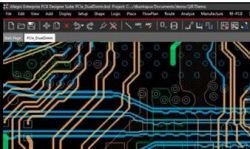
Cadence PCB - это простое и практичное программное обеспечение для проектирования PCB, которое может выполнять проектирование принципиальных диаграмм и создание символов принципиальных диаграмм.
2023-07-10
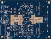
Конструкция PCB основана на принципе схемы для выполнения функций, необходимых дизайнеру схемы.
2022-11-22
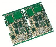
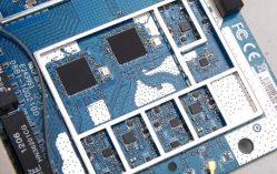
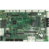
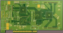
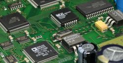
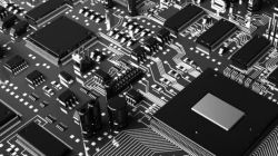
Плата PCB является основным компонентом электроники, и любая электроника требует создания платы PCB.
2022-01-27
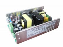
После завершения проектирования проводки PCB переключателя питания необходимо тщательно проверить, соответствует ли конструкция проводки правилам, установленным дизайнером.
2022-01-02
Из - за увеличения частоты чистое сопротивление металлического проводника увеличивается с увеличением сопротивления. Это связано с тем, что магнитное поле делает передачу тока все более склонной к металлической поверхности.
2021-12-31
Рекомендации включают в себя все конфигурации полос и микрополос для управления сопротивлением. Подумайте об объединении ваших прогнозов сопротивления с прогнозами производителей PCB - панелей.
2021-12-28
Do not place the crystal oscillator on the edge of the PCB board. Pay special attention to this point when designing the PCB board.
2021-12-27
При проектировании печатных плат обратный дизайн может быть реализован путем стратификации, разумной компоновки и установки.
2021-12-15
Я буду обсуждать основные правила монтажа и компоновки компонентов в панелях PCB , для новых сотрудников, занимающихся разработкой PCB.
2021-12-14
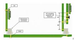
Общей проблемой SI является отражение, и мы знаем, что линии передачи PCB - пластины имеют характеристики « характеристического сопротивления».
2021-12-13
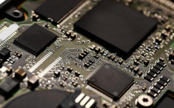
PCB design is pointer to circuit board design. Printed circuit board design is based on circuit schematic diagram, circuit designers need to achieve the function.
2021-12-09
7 good habits of PCB layout engineers. Let's see how many you have! Good PCB layout working habits benefit you a lot.
2021-11-11
принципиальная ошибка схемы репликации платы PCB 1. обычная ошибка в схеме PCB: (1) Нет сигнала...
PCB material selection is the first step in the PCB design process. Choosing the right material for your design is very ...
Когда сигнал передается от источника к нагрузке через проводник PCB, он проходит через затухание.
При выборе материала PCB важно сделать правильный выбор для вашего дизайна, потому что материал влияет.
разработка электронных продуктов PCB является относительно сложной задачей. Она должна быть тщательно спланирована, чтобы достичь результата
как и во многих технологиях электронной промышленности, панелей PCB имеют множество возможностей и вариантов. Потому что каждый раз, чтобы сделать...
Here is an overview of some methods, materials, software, and tools that can be used to produce PCBs, and hope it will h...
When building electronic circuit boards, design integrity must be maintained throughout the process. PCBA developmen...