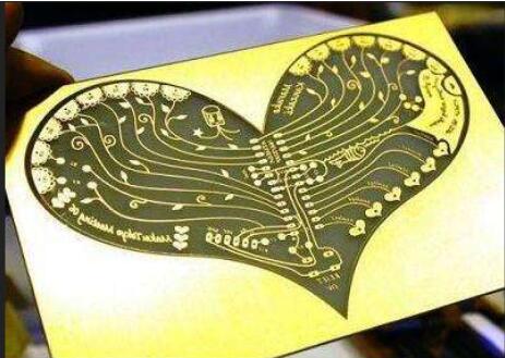
Super difficult Four-sided carbon fiber body This will be a very difficult process. сначала, let's listen to what kind of ideas the Azumino factory of VAIO headquarters has to manufacture products. чистая вода: наша цель - производство продукции, на которую покупатель может положиться. VAIO has always attached great importance to the trust relationship with customers. This relationship is measured by the manufacturer through sensory testing (using human vision, осязание и другие чувства. Detection) or manual assembly. In addition, we also design and ensure stable production of small equipment (a general term for components that can support the processing and assembly of components) and large equipment such as presses. наше главное преимущество - обеспечить стабильное качество работы., ultra-high precision and various We believe that using the respective strengths of humans, машина and equipment to improve production quality is closely related to winning the trust of customers.

Chip packaging
BGA (ballgridarray) BGA package physical [1] ball contact array, герметизация поверхности. On the back of the printed circuit board, в режиме отображения появятся Шаровые выступы, которые заменят пятки, кристалл LSI собран на лицевой стороне печатной платы, затем уплотнение через формовочную смолу или уплотнение. Also known as bump display carrier (PAC). количество иголок может превышать 200, which is a package for multi-pin LSI. The package body can also be made smaller than QFP (Quad Flat Package). например, центрирование выводов для 1360 штырей BGA.5mm is only 31mm square; while a 304-pin QFP with a pin center distance of 0.5 мм - квадрат 40 мм. And BGA does not have to worry about pin deformation like QFP.
Layout line width and spacing traces teardrop vias [6 details to quickly improve the quality of PCB boards]
Preface Now many PCBLAYUT - инженер завершил компоновку и проводку в соответствии с правилами, волочильный станок. If you don't want to be treated as a "wire puller". иметь определённое представление о цепи, иметь возможность делать пи/SI - анализ/PI engineers. PCBLAYUt is a technical job, but also an experience job. усвоение некоторых полезных уроков часто приносит большую пользу. схема PCBструктурная схема, literally explained, рациональное расположение элементов цепи.