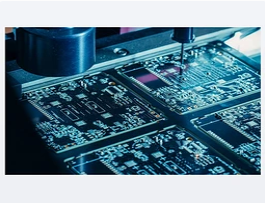
In the process of PCB design and production, инженерам нужно не только предотвращать аварию в процессе строительства PCB - производство, but also need to avoid design errors. В настоящем документе обобщаются и анализируются эти общие проблемы PCB, hoping to bring some help to everyone's design and production work.
Вопрос 1: панель PCB short circuit
This problem is one of the common faults that will directly cause the панель PCB не работать. There are many reasons for this problem. Давайте поочередно проанализируем.
The biggest cause of PCB short circuitis improper solder pad design. сейчас, the round solder pad can be changed to an oval shape to increase the distance between points to prevent short circuits.
неправильное проектирование компонентов PCB по направлению также может привести к короткому замыканию платы и невозможности работать. например, if the pin of the SOIC is parallel to the tin wave, легко привести к короткому замыканию. сейчас, the direction of the part can be appropriately modified to make it perpendicular to the tin wave.
Еще один возможный сбой, приводящий к короткому замыканию PCB, that is, автоматический модуль искривил ногу. Поскольку IPC устанавливает длину штифта менее 2 мм, и опасается, что при слишком большом углу искривления опоры деталь может упасть, короткое замыкание, and the solder joint must be more than 2mm away from the circuit.
три причины, there are also some reasons that can cause short-circuit failures of the панель PCB, например, дыра на плите, too low temperature in the tin furnace, ошибка свариваемости платы, отказ сварочного фотошаблона, and board Surface pollution, сорт., are relatively common causes of failures. инженеры могут сравнивать вышеуказанные причины с обстоятельствами неисправности, устранять и проверять каждый раз.
Вопрос 2: на панелях PCB видны темные и зернистые контакты
The problem of dark color or small-grained joints on the панель PCB в основном из - за загрязнения припоя и избыточного оксида в смеси расплавленного олова, какой вид сварной точки структура слишком хрупкая. Be careful not to confuse it with the dark color caused by the use of solder with low tin content.
Другая причина этого - изменение состава припоя, используемого в производстве., and the impurity content is too high. необходимо добавить чистое олово или заменить припой. The stained glass causes physical changes in the fiber build-up, например, между слоем и слоем. But this situation is not due to poor сварная точка. причина в перегреве основной пластины, and it is necessary to reduce the preheating and soldering temperature or increase the speed of the substrate.
Problem three: PCB solder joints become golden yellow
Under normal circumstances, the solder on the панель PCB Он серебристый, but occasionally there are golden solder joints. главная причина этого - слишком высокая температура.. At this time, Вам нужно только понизить температуру олова.
Question 4: The bad board is also affected by the environment
Due to the structure of the PCB itself, когда PCB находится в неблагоприятных условиях, его легко повредить. Extreme temperature or temperature fluctuations, избыточная влажность, high-intensity vibration and other conditions are all factors that cause the board's performance to decrease or even scrap. например, changes in ambient temperature will cause deformation of the board. поэтому, the solder joints will be destroyed, форма листа будет изгибаться, or the copper traces on the board may be broken.
С другой стороны, moisture in the air can cause oxidation, коррозия и ржавчина металлических поверхностей, such as exposed copper traces, solder joints, pads, & компонент. Accumulation of dirt, пыль или обломки поверхности агрегатов и платы также уменьшают поток и охлаждение агрегатов, causing PCB overheating and performance degradation. вибрация, falling, удар или изгиб PCB может деформировать и вызвать трещины, при высоком токе или перенапряжении возникает сбой PCB, или приводит к быстрому старению компонентов и пути.
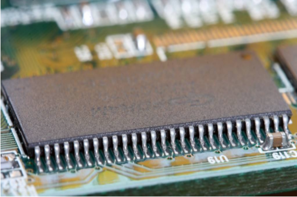
Problem five: PCB open circuit
When the trace is broken, или когда припой находится только на паяльном диске, а не на проводе элемента, an open circuit can occur. В таком случае, there is no adhesion or connection between the component and the PCB. как короткое замыкание, these may also occur during the production process or during the welding process and other operations. вибрация или растяжение платы, dropping them or other mechanical deformation factors will destroy the traces or solder joints. так же, chemical or moisture can cause solder or metal parts to wear, Это может привести к разрыву проводов сборки.
Problem six: loose or misplaced components
During the reflow soldering process, маленькие детали могут плавать на плавленном припое, в конце концов, покинуть цель точки сварки. возможные причины перемещения или наклона включают вибрацию или отскок сварных поверхностных сборок панель PCB due to insufficient circuit board support, установка возвратной печи, solder paste вопрос, ошибка.

Problem seven: welding problem
The following are some of the problems caused by poor welding practices:
Disturbed solder joints: The solder moves before solidification due to external disturbances. Это похоже на точку холодной сварки, but the reason is different. можно исправить за счет подогрева, and the solder joints are not disturbed by the outside when they are cooled.
холодная сварка: это происходит, когда припой не плавится правильно, вызывать шероховатость поверхности и ненадежность связи. слишком много припоя остановит полную плавку, может также появиться температура. The remedy is to reheat the joint and remove the excess solder.
мост припоя: это происходит при пересечении и физическом соединении двух проводов. Это может создавать случайное соединение и короткое замыкание, which may cause the components to burn out or burn out the traces when the current is too high.
паяльная тарелка: недостаточно увлажняющий свинец или свинец. слишком много или слишком мало припоя. Pads that are elevated due to overheating or rough soldering.
Problem eight: human error
Most of the defects in PCB - производствоare caused by human error. В большинстве случаев, wrong production processes, неправильное размещение компонентов и непрофессиональные нормы изготовления могут привести к до 64% предотвратимых дефектов продукции. из - за следующих, the possibility of defects increases with the complexity of the circuit and the number of production processes: densely packaged components; multiple circuit layers; fine wiring; surface soldering components; power and ground planes
Although every manufacturer or assembler hopes that theпанель PCB produced is free of defects, but there are so many design and production process problems that cause continuous панель PCBproblems.
Typical problems and results include the following points: poor soldering can lead to short circuits, разомкнутая цепь, cold solder joints, сорт.; misalignment of the board layers can lead to poor contact and poor overall performance; poor insulation of copper traces can lead to traces and traces There is an arc between the wires; if the copper traces are placed too tightly between the vias, существует риск короткого замыкания; недостаточная толщина платы может привести к изгибу и разрушению.