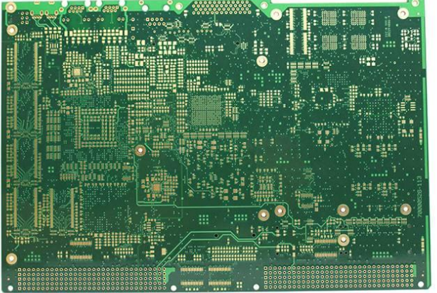
числовое перемешивание мод рисунок PCB
1. Understanding the basic concepts of digital-analog hybrid design
Many products include mixed digital-analog проектирование PCBs, and different signals have different anti-interference capabilities. в процессе проектирования межсоединений, the crosstalk between different signals must be reasonably controlled in order to ensure the index requirements of the final product.
очень важно понять следующие основные понятия. Mastering the basic concepts of digital-analog hybrid design will help understand the strict layout and прокладка проводов design rules that will be formulated later, Таким образом, при проектировании гибридной энергии для нескольких мод конечный продукт не будет легко сделать скидку. Implement the important constraint rules. Это помогает гибко и эффективно решать проблемы последовательности, которые могут возникать в цифровых аналоговых схемах смешанный дизайн.
1. The important difference between analog signal and digital signal in anti-interference ability
The digital signal level has a strong anti-interference ability, и меньше помехоустойчивости аналоговых сигналов.
например, a триV level digital signal can tolerate even a 0.3V последовательный сигнал, не влияющий на логическое состояние. Однако, in the field of analog signals, некоторые сигналы очень слабы. например, чувствительность мобильных телефонов GSM к приему может достигать - 110dBm, which is only equivalent to an effective value of a sine wave of 0.7uv. шум интерференции в диапазоне uv, даже при входе в верхнюю часть LNA, Это достаточно для значительного снижения чувствительности станции к приему. This slight interference may come from small noises on the digital control signal line or power ground line.
с точки зрения системы, digital signals are generally only transmitted on the board or in the frame. For example, memory bus signals, авиагоризонта управления мощностью, сорт., as long as it is ensured that the interference received from the sending end to the receiving end is not enough to affect the judgment of the logic state. аналоговый сигнал должен быть модулирован через ряд процессов, frequency conversion, увеличить, transmission, пространственное распространение, reception, демодулировать перед восстановлением. During this process, сигнал непрерывного снижения шума. с точки зрения системы, it is necessary to ensure that the final signal-to-noise ratio meets the requirements in order to demodulate correctly. максимальное затухание и шум от пространственного распространения. In order to achieve better communication performance, необходимо свести к минимуму помехи при соединении на платы.
поэтому, можно считать, что требования к последовательному вмешательству аналоговых сигналов в десятки раз выше, чем требования к последовательному вмешательству цифровых сигналов., and may even reach tens of thousands of times.

2. High-precision ADC and DAC circuits
In an ideal situation, the relationship between the signal-to-noise ratio of linear ADC and DAC circuits and the number of conversion bits is:
SNR=10Log(F2/N2)=10Log[A2/2/(A2/3Ã2n)]=6.02n+1.76 dB
For 14-bit linear ADCs and DACs, if the least significant bit (LSB) is valid, the theoretical signal-to-noise ratio can be calculated to be 86dBc. по сравнению с требованиями цифровой схемы, the high-precision 14-bit linearity The noise requirements of ADCs and DACs are at least 1000 times higher than that of digital signals. Конечно, if only 11 bits are required for the least significant number of bits, требование о последовательном вмешательстве может быть снижено, but it is still much higher than the requirement for digital signals.
Эти две ситуации в примечании указывают на то, что аналоговые схемы в мультимодовых смешанных одинарных панелях очень уязвимы для помех, which will affect the signal-to-noise ratio and other indicators. Therefore, in the process of digital-analog hybrid single-boardпроектирование PCB, необходимо предъявлять очень высокие требования к планировке и монтажу.
3. Digital signal is a strong source of interference to analog signal
The level of the digital signal is very high compared to the analog signal, частота гармоник в цифровых сигналах, Поэтому цифровые сигналы сами по себе являются мощным источником помех для аналоговых сигналов. In particular, большой ток часовой сигнал и выключатель питания является одним из нескольких типов смеси дизайн, чтобы обратить внимание на сильные сухие возмущения.
4. The fundamental purpose of digital-analog hybrid interconnection design
We can understand the digital-to-analog design problem in this way. цифровая схема, Мы следуем правилам проектирования цифровых схем. In the area of digital circuits, можно разрешить большие помехи, as long as it does not affect the implementation of system functions and external emc indicators.
то, что мы здесь называем "больше" относительно аналоговой схемы. For digital circuits, it is not necessary and impossible for us to control the existence of crosstalk like analog circuits. аналоговая схема, we must follow the design rules of analog circuits, допустимые помехи в области аналоговых схем гораздо меньше, чем в области цифровых схем.
The purpose of digital-analog hybrid interconnection design is to ensure that the interference of digital signals only exists in the digital signal area through reasonable layout, wiring, shielding, фильтровать, and power supply division.
Мы должны обратить внимание на источник помех, чувствительный контур, & путь помех. Ниже описываются принципы компоновки и проводки, используемые в этих трех областях.. Successful digital-analog hybrid single-board design must be realized with careful attention to every step and every detail in the entire process. Это означает, что в начале проектирования необходимо тщательно и тщательно спланировать, and every design step must be carefully planned. прогресс в этой работе оценивается на всеобъемлющей и постоянной основе. The layout and routing must be carefully checked and verified to ensure 100% compliance with the layout and routing rules. иначе, improper routing of a signal line will completely destroy an otherwise very good circuit board.
правила устарели.. Only through a deep understanding of the rules can we ensure that we can use the rules correctly and complete an excellent design.
второй, the circuit type distinction
Before explaining the layout rules of digital-analog hybrid design, Теперь мы будем различать источник помех, sensitive circuits and interference paths on the terminal board. понимание этих источников помех и чувствительных схем поможет нам правильно планировать компоновку и проводку. Understanding is essential.
1. Analog circuit
For end products, аналоговая схема включает все радиочастотные схемы, radio frequency power supplies, канал радиочастотного управления, digital-to-analog conversion circuits, схема суммы звука. All of the above analog circuits are sensitive circuits. среди, sensitive circuits that need special attention include frequency termination circuits (including local oscillator signals, frequency synthesis circuit power and control signals), receiving front-end circuits, схема суммы звука.
2. Sources of interference
Interference sources include all digital circuits, high-power radio frequency circuits (power amplifiers, antennas and other high-power radio frequency circuits). среди, the interference sources that need special attention include clock circuits, коммутационное питание, силовая линия большого тока, power amplifier circuits, антенная цепь. The interference of radio frequency signals such as power amplifiers and antennas is analyzed in the radio frequency design part of this specification.
3. Interference path
The interference paths that need to be paid attention to for digital-analog hybrid design include: space radiation, power ground (plane or wiring), digital-to-analog conversion circuits, различные управляющие сигналы аналоговой схемы.
(1) Space radiation: The circuits that are close to each other will generate crosstalk through radiation, Это то же самое, что и понятие последовательности цифровых сигналов., but it should be noted that the crosstalk that analog signals can tolerate is much smaller than that of digital signals, Поэтому необходимо управлять последовательными помехами на этапе компоновки. уменьшение пространственного излучения обычно путем удлинения схемы и использования экранирующей коробки.
(2) Power ground: The power ground is a common loop between digital and analog circuits, Таким образом, сигнал помехи может передаваться через заземляющий проводник питания чувствительным контурам. The way to control the crosstalk of the power supply ground is to use filter components and power supply ground division reasonably.
(3) Digital-to-analog conversion circuit: It is an interface between analog and digital signals. If the layout or wiring is handled improperly, например, схема с цифровыми и аналоговыми схемами не ясна, проводки перекрещиваются, it may cause crosstalk.
(4) Analog control signal: The ideal analog device should be that the control signal and the analog circuit are isolated inside the device, управляющий сигнал должен обеспечивать только правильность логического уровня. However, такие устройства обычно не могут этого сделать, and the interference number on the control signal may be directly coupled to the analog circuit. Решение заключается в сведении к минимуму помех сигналов управления аналоговыми схемами, рациональном использовании фильтрующих элементов.