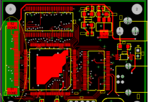
5 basic проектирование PCB стандарт you have to see
For many проектирование PCB новичок, understanding the most basic specifications of проектирование PCB Это главная задача., Это будет способствовать развитию проектирование PCB habits and be more suitable for all aspects of electronic manufacturing, например производство PCB, SMT chip processing, модуль DIP, etc. пять основных норм изложены ниже. проектирование PCB до нитки.
1. Shielding cover design
The distance between the shielding cover and the shielding cover and between the components in the shielding cover and the shielding cover must be greater than 0.4MM
Reason: сейчас, the width of the shielding cover pad is 0.7 мм. In order to reduce the problem of false welding of the shielding cover, в частности, для типов, оснащенных многими экранирующими крышками и главным образом фасонным оборудованием, the corners of the shielding cover are easily welded. At present, the shielding cover is welded. ширина стальной сетки
0.3mm-0.5mm внутренняя и внешняя развёртка

The pad of the shield cover should not be too long, Потому что длина прокладки слишком длинная, крышка экранирования и зигзагообразная сварка, which will cause local virtual welding. длина прокладки крышки составляет 2 - 2 дюйма.5 мм, высота пилы 0.3MM-0.5 мм. For the bending part, Рекомендуемая длина прокладки 1 мм.2-1.5 мм. The shielding cover pin needs to be made into a serrated shape. согласование с подкладкой.
Reason: The current требования for shielding cover manufacturers are: the deformation range of 0.1 мм нормально, and the deformation position often appears in the bending part. Плюс Наша текущая толщина сетки 0.12mm, трудно освоить сварочный эффект штифта, and The larger the pad, Чем меньше количество флюса на паяльном диске.
2. The pad spacing between PCB devices
The pad spacing between devices must meet the most basic проектирование PCB requirements.
The distance between the discharge tube and the adjacent component PAD>0.3mm (the distance between the discharge tube and the adjacent component PAD, the same network>0.15 мм, different networks>0.2mm) The distance between the discharge tube and the discharge tube>0.1 mm
3. Process clamping edge
The craft edge distance from the top of the veneer>5MM (Note: the machine clamp to the craft edge is 4.5MM) The width of the craft clamping edge>4MM During the PCB mounting process, PCB должна быть на определенной границе, чтобы зажимать. Within this range, нельзя помещать узлы и прокладки. In case of high-density boards, зажим края не может остаться, the process edges can be designed or the panel form can be used. ширина зависит от выбранной ширины SMT equipment. В общем, the process margin is 6.0 мм от верхней части блока или от края одной пластины, that is, the process margin is closest to the top of the component or >5mm from the PCB inner board.
4. MARK point design
In the design of the MARK points of the PCB board, the MARK points on the same surface are designed to be symmetrical (the left and right MARK points are the same distance from the board edge), and the upper and lower MARK points are asymmetric (the upper and lower MARK points are different from the board edge). ждать встречи. The diameter of the MARK point on the PCB board is 1.0 мм.
5. установочное отверстие
во всей панеле установочные отверстия имеют диаметр 2,5 мм + - 0,1 мм, а компоненты не расположены в пределах 1 мм вокруг отверстия для определения местоположения, с тем чтобы избежать наддува крепежных обсадных колонн при работе на поддонах.
требования к отверстиям для установки фундамента в одной панели: текущий стандарт: 3. 0MM-3.8MM
The above are the basic проектирование PCB specifications, which are suitable for beginners and must be mastered and used. На самом деле, проектирование PCB specifications are far more than these. Конструктору нужно постоянно подытоживаться в сложной работе., обеспечение того, чтобы основные принципы были продиктованы производительностью и ясностью проектирование PCB documents sent out are accurate, ясно. это тоже передовой метод. проектирование PCB. An important aspect of the gap between engineers and beginners.