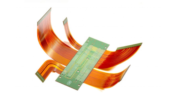
The so-called copper pour is to use the unused space on the flexible circuit board as a reference surface and then fill it with solid copper. Эти медные области также называют медными наполнителями. The significance of copper coating is to reduce the impedance of the ground wire and improve the anti-interference ability; reduce the voltage drop and improve the efficiency of the power supply; connecting with the ground wire can also reduce the loop area. также для того, чтобы PCB не деформировался во время сварки, most Производители PCB Необходимо также, чтобы дизайнеры PCB заполняли открытые зоны PCB медными или сетчатыми линиями. If the copper is not handled properly, она определит, является ли прибыль или потеря стимулом или потерей, is the copper coating "the advantages outweigh the disadvantages" or "the disadvantages outweigh the advantages"?
Все знают под высокой частотой, the distributed capacitance of the wiring on the printed circuit board will play a role. когда длина больше 1/20 of the corresponding wavelength of the noise frequency, будет эффект антенны, and the noise will be emitted through the wiring. если в PCB есть заземленная медь, the copper pour becomes a tool for spreading noise. поэтому, in a high-frequency circuit, не считай заземление заземлением. This is the "ground "Line", Должно быть меньше чем '/20, перфорация на проводе, and "good ground" with the ground plane of the multilayer board. Если медное покрытие правильно обработано, the copper coating not only increases the current, также играет двойную роль экранирующих помех.

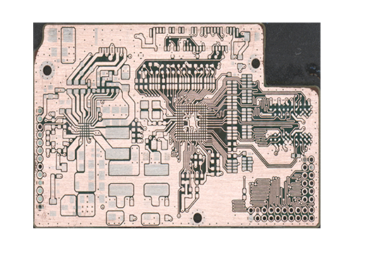
There are generally two basic methods for copper coating, крупная медь и сетка меди. It is often asked whether large-area copper coating is better than grid copper coating. В любом случае плохо. Но почему?? Large-area copper coating has the dual functions of increasing current and shielding. Однако, if large-area copper coating is used for wave soldering, плата может быть поднята, даже пузырь. поэтому, for large-area copper coating, обычно используется несколько пазов для облегчения вспенивания медной фольги. медное покрытие чистой сетки используется в основном для защиты, увеличение эффекта тока также снижает эффект. From the perspective of heat dissipation, the mesh is beneficial (It lowers the heating surface of the copper) and plays a role of electromagnetic shielding to a certain extent.
медный лист следующего типа питания не может использоваться в сети
Следует отметить, что сетка состоит из диагональных дорожек. Мы знаем про PCB - схему, the width of След PCB has a corresponding "electrical length" (actual size) for the operating frequency of the circuit board. частота чисел, соответствующая рабочей частоте, См.. When the working frequency is not very high, Возможно, роль сетки не очень заметна. Once the electrical length matches the working frequency, Это будет очень плохо. вы обнаружите, что схема не работает нормально, and signals that interfere with the operation of the system are being emitted everywhere. Так что для коллег, использующих сетку, my suggestion is to choose according to the working conditions of the designed circuit board, Не упорствуй в одном. Therefore, высокие требования к помехоустойчивости высокочастотных схем к многоцелевой сети, and low-frequency circuits have circuits with large currents, как цельная медь.