с быстрым развитием электронной техники, only by recognizing the development trend of PCB technology, circuit board manufacturers can actively develop and innovate production technology in order to find a way in the fiercely competitive PCB industry. Производители плат должны всегда поддерживать сознание развития. The following are some views on the development of PCB production and processing technology in Changsha:
1. Develop component embedding technology
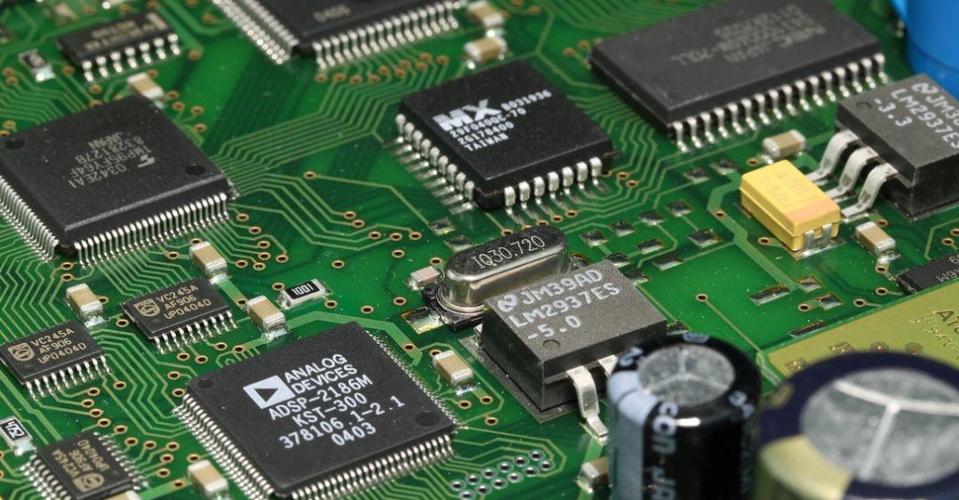
Component embedding technology is a huge change in PCB functional integrated circuits. The formation of semiconductor devices (called active components), electronic components (called passive components) or passive components on the inner layer of the PCB has begun. производство, but to develop circuit board manufacturers must first solve the analog design method, production technology and inspection quality, reliability assurance is also a top priority. завод по производству панелей PCB в чанше должен увеличить инвестиции в системные ресурсы, включая проектирование, устройство, testing, чтобы сохранить живучесть.
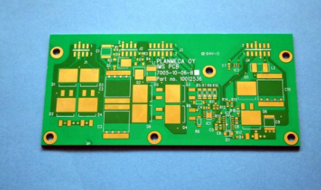
Several major trends in the development and innovation of PCB technology in завод платы
2. HDI pcb technology is still the mainstream development direction
HDI pcb technology promotes the development of mobile phones, drives the development of information processing and control basic frequency functions of LSI and CSP chips (packages), and the development of template substrates for circuit board packaging. It also promotes the development of PCBs. Therefore, circuit board manufacturers must follow the HDI road Innovate PCB production and processing technology. As HDI embodies the most advanced technology of contemporary PCB, Он приносит тонкие нитки и маленькие отверстия для панелей PCB.. HDI multi-layer board application terminal electronic products-mobile phones (mobile phones) is a model of HDI cutting-edge development technology. в телефоне, PCB motherboard micro-wires (50μmï½75μm/50μmï½75μm, wire width/spacing) have become the mainstream. In addition, тонкий проводящий слой и толщина пластины; рисунок электропроводности утончен, which brings high-density and high-performance electronic equipment .

3. непрерывно заимствовать передовое производственное оборудование, обновить изготовление платыprocess
HDI manufacturing has matured and tends to be perfected. развитие технологии PCB, although the commonly used subtractive manufacturing methods in the past still dominate, low-cost processes such as additive and semi-additive methods have begun to emerge. Using nanotechnology to make holes metallized and simultaneously form PCB conductive patterns, a novel manufacturing process method for flexible boards. высокая надежность, high-quality printing method, inkjet PCB process. Production of fine wires, новый тип светомаски высокого разрешения и экспонирования, and laser direct exposure devices. Uniform plating equipment. Production component embedded (passive active component) manufacturing and installation equipment and facilities.
Several major trends in the development and innovation of PCB technology in завод платы
4. Develop higher performance PCB raw materials
Whether it is a rigid PCB circuit board or a flexible PCB circuit board material, Глобализация неэтиленовых электронных продуктов, these materials must be required to have higher heat resistance, so the new type of high Tg, малый коэффициент теплового расширения, small dielectric constant, а потери диэлектрика все больше и больше, появляется высококачественный материал.
5. Bright prospects for photoelectric PCB
The photoelectric PCB circuit board uses the optical path layer and the circuit layer to transmit signals. The key to this new technology is to manufacture the optical path layer (optical waveguide layer). It is an organic polymer that is formed by methods such as flat plate photocopying, лазерная абляция, and reactive ion etching. сейчас, this technology has been industrialized in Japan and the United States. как главный производитель, Chinese PCB manufacturers should also actively respond and keep up with the pace of scientific and technological development.