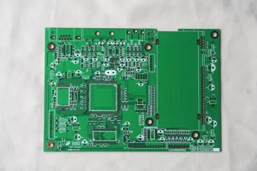
Proofing процесс of multi-layer pcb circuit board
With the rapid development of automotive electronics, communication electronics, промышленный контроль, instrumentation, медицинская электроника, авиационно - космическая и другие отрасли промышленности, the многослойная плата PCBпромышленность также время от времени удовлетворяет потребности рынка и потребителей, and promotes the rapid increase in industry output value from time to time However, the competition in the multi-layer PCB circuit board industry is increasing. многие производители платы без колебаний снижают цены, преувеличивают потребление, чтобы привлечь большое число клиентов. However, низкая цена pcb пластины должны использовать низкий материал, which affects the quality of production, короткий срок службы, and the product is prone to appearance damage, болтанка и другие вопросы массы.
The purpose of multi-layer выборка платы PCBчтобы определить сильные стороны производителя потребительских товаров, можно эффективно снизить нежелательность многослойных панелей PCB, заложить прочную основу для будущего народного потребления. Let's look at the multi-layer выборка платы PCBprocess.
Multilayer выборка платы PCBprocess:
One, contact the circuit board manufacturer
First of all, you need to notify the manufacturer of the documents, выполнять просьбу, and quantities. "какие параметры необходимы для пробоотбора многослойной схемы PCB?"?" Order, следить за графиком потребления.
Second, open material
Purpose: According to the request of the engineering materials MI, разрезать большой лист бумаги, удовлетворяющий требованиям заказчика, на мелкие кусочки бумаги.
Process: large sheet cutting board according to MI request curb board beer fillet\grinding board out
Three, drilling
Purpose: According to the engineering materials, бурение необходимого отверстия на соответствующем месте на доске, отвечающей требуемому размеру.
process: stacked plate pin upper plate drilling lower plate inspection\repair
Four, Shen copper
Purpose: Copper sinking is the application of chemical methods to deposit a thin layer of copper on the wall of the insulating hole.
process: rough grinding hanging board automatic copper immersion line lower board dip 1% dilute H2SO4 thickened copper

Five, graphics transfer
Purpose: Graphic transfer is to transfer the image on the consumer film to the board.
Process: (blue oil process): grinding plate printing the first side drying printing the second side drying exploding shadowing inspection; (dry film process): hemp board pressing film standing right Position Exposure Standing Development Check
VI. Graphic plating
Purpose: Pattern electroplating is to electroplate a copper layer with the required thickness and a gold-nickel or tin layer with the required thickness on the exposed copper skin of the circuit pattern or the hole wall.
process: upper board degreasing second water washing micro-etching water washing pickling copper plating water washing pickling tin plating water washing lower board
ä¸Remove the film
Purpose: Use NaOH solution to remove the anti-electroplating masking layer to expose the non-circuit copper layer.
Process: water film: insert rack soak alkali rinse scrub pass machine; dry film: release board pass machine
8. Etching
Purpose: Etching is to use chemical reaction to corrode the copper layer of non-circuit parts.
девять, green oil
Purpose: Green oil is to transfer the graphic of the green oil film to the board to maintain the circuit and prevent the tin on the circuit when welding parts.
process: grinding plate printing photosensitive green oil curium plate exposure developing; grinding plate printing the first side drying plate printing the second side drying plate
åCharacter
Purpose: Characters are provided as a mark for easy identification.
Process: After the green oil finishes cool and stand adjust the screen print characters back
eleven, gold-plated fingers
1. назначение: покрытие никелем/gold with the required thickness on the plug finger to make it more hard and wear-resistant.
process: upper plate degreasing washing twice micro-etching washing twice pickling copper plating washing nickel plating washing gold plating
2, tin plate (a process in parallel)
Purpose: Tin spraying is to spray a layer of lead tin on the exposed copper surface that is not covered by solder mask to protect the copper surface from corrosion and oxidation to ensure good soldering performance.
process: micro-erosion air drying preheating rosin coating solder coating hot air leveling air cooling washing and air drying
12. Forming
Purpose: Organic gongs, пивоварня, hand gongs, ручная резка может производиться с помощью штамповочных или цифровых режущих машин.
уточнение: данные по машинным и пивным плитам более точны, гонг второй, а минимальная ручная режущая плита может быть сделана только в простой форме.
- 13.... Test
Purpose: After electronic 100% testing, обнаружение дефектов, such as open circuits and short circuits that are not easy to find visually.
Process: upper mold release board test pass FQC visual inspection unqualified repair return test OK REJ scrap
Fourteen, final inspection
Purpose: After 100% visual inspection of board appearance defects, and stop repairing minor defects to prevent problems and defective boards from flowing out.
детальный рабочий процесс: входящий материал - просмотр материалов - визуальный осмотр - проверка соответствия - выборочная проверка FQA - проверка соответствия - упаковка - неудовлетворительное состояние - удаление - проверка OK!
из - за высокого технического содержания конструкции, обработка и изготовление многослойных мембран Производители панелей PCB. поэтому, as long as every detail of PCB proofing and manufacturing is done accurately and rigorously, Доступ к высококачественным PCB - продуктам. выигрывать больше клиентов, выигрывать больше рынка.