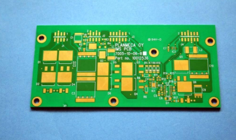
Common PCB surface treatment process
Foreword: многослойная плата PCBтехнология обработки поверхности означает искусственное образование слоя поверхности, отличного от механического соединения компонентов PCB и электрических узлов, physical and chemical properties of the substrate. Цель заключается в том, чтобы обеспечить хорошую свариваемость или электрические характеристики PCB.. Потому что медь часто присутствует в воздухе в виде оксида, серьезное влияние на свариваемость и электрические характеристики PCB, it is necessary to perform surface treatment on the PCB multilayer circuit board.
The common surface treatment methods are as follows:
1, hot air leveling
The process of coating molten tin-lead solder on the surface of the PCB and flattening (flattening) with heated compressed air to form a coating layer that is resistant to copper oxidation and provides good solderability. в процессе выравнивания горячего дутья, the solder and copper form a copper-tin metal compound at the junction, and the thickness is about 1 to 2 mils;
2, chemically immersed nickel gold
A thick layer of nickel-gold alloy with good electrical properties is wrapped on the copper surface and can protect the PCB for a long time. Не похоже на OSP, which is only used as an anti-rust barrier layer, в процессе долгосрочного использования PCB, он может быть полезен для достижения хороших электрических свойств. Кроме того, it also has tolerance to the environment that other surface treatment processes do not have;
3, chemical immersion silver
Between OSP and electroless nickel/пропитка золотом, the process is simpler and faster. при высокой температуре, humidity and pollution, Он по - прежнему может обеспечивать хорошие электрические характеристики и сохраняет хорошую свариваемость, Но она будет тускнеть. Because there is no nickel under the silver layer, физическая прочность погружения серебра лучше химического никелирования/immersion gold;

4, organic anti-oxidation (OSP)
On the clean bare copper surface, a layer of organic film is grown chemically. Эта плёнка имеет устойчивость к окислению, heat shock resistance, and moisture resistance to protect the copper surface from rusting (oxidation or sulfidation, сорт.) in a normal environment; at the same time, it must be easily assisted in the subsequent welding high temperature The flux is quickly removed to facilitate welding;
5, electroplating nickel gold
The conductor on the PCB surface is electroplated with a layer of nickel and then electroplated with a layer of gold. Основная цель никелирования - предотвратить распространение золота и меди. There are two types of electroplated nickel gold: soft gold plating (pure gold, gold indicates that it does not look bright) and hard gold plating (the surface is smooth and hard, wear-resistant, кобальт и другие элементы, and the surface looks brighter). Soft gold is mainly used for gold wire during chip packaging; hard gold is mainly used for electrical interconnection in non-soldering places (such as gold fingers).
..., многослойная плата PCBmixed surface treatment technology
Choose two or more surface treatment methods for surface treatment. The common forms are: Immersion Nickel Gold + Anti-oxidation, Electroplating Nickel Gold + Immersion Nickel Gold, Electroplating Nickel Gold + Hot Air Leveling, Immersion Nickel Gold + Hot Air Leveling .
во всех методах обработки поверхности, hot air leveling (lead-free/leaded) is the most common and cheapest treatment method, Но обратите внимание на правила ЕС в отношении RoHS.
RoHS: RoHS is a mandatory standard established by EU legislation. Its full name is "Restriction of Hazardous Substances" (Restriction of Hazardous Substances). The standard has been officially implemented on July 1, 2006 год, and is mainly used to standardize the material and process standards of electrical and electronic products, Укрепление здоровья человека и охрана окружающей среды. The purpose of this standard is to eliminate six substances including lead, Меркурий, cadmium, шестивалентный хром, polybrominated biphenyls and polybrominated diphenyl ethers in electrical and electronic products, и уточняет, что содержание свинца не должно превышать 0.1%.
IPcb - Высокотехнологичное предприятие, специализирующееся на разработке и производстве высокоточного PCB. iPCB is happy to be your business partner. наша цель – стать самым профессиональным прототипомПроизводители PCBв мире. Mainly focus on microwave high frequency PCB, давление смешения высоких частот, ultra-high multi-layer IC testing, from 1+ to 6+ HDI, Anylayer HDI, основа интегральной схемы, IC test board, жёсткий лист, ordinary multi-layer FR4 PCB, etc. Products are widely used in industry 4.0, связь, industrial control, цифровой, power, компьютер, automobiles, медицинский, aerospace, прибор, Internet of Things and other fields.