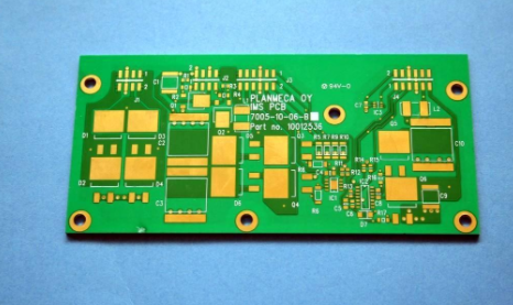
Multi-layer circuit board "via hole cover oil" and "via hole opening window" are silly and unclear
Regarding этот "through-hole opening" and "through-hole cover oil" of многослойная плата PCB((различие в употреблении между PAD и VIA)), многие клиенты и инженеры - Дизайнеры часто спрашивают поставщиков при покупке платы. Мне нужно сделать "отверстие для прохода" или "масло для крышки для прохода". сейчас, У многих покупателей могут возникнуть сомнения. What does this mean? какой параметр я должен выбрать в файле? The description of this problem is as follows:
I often encounter such problems. неправильное проектирование файла, and it is difficult to distinguish which is the pad of the PCB multi-layer circuit board and which is the use of via. Иногда электропроводное отверстие обрабатывается свойствами паяльного диска, Иногда используется атрибут ключа. Разберись с этим., the design of VIA attributes and PAD attributes is confusing, Ошибка обработки, which is also one of the problems that often appear complaints. применимый к производителю платы, при обработке данных CAM, some film processing engineers will make mistakes because the customers design documents are not standardized. изредка, some engineers will help customers modify the documents and make the non-standard design right. мой собственный опыт обработки инженерных данных, this has led to and contributed to the non-standard design of customers.

В прошлый раз ты поступил правильно., Это не значит, что файл правильный! All engineers must pay attention to the design standards and specifications. требовать, чтобы все инженеры по обработке фильмов поддерживали текущий статус файлов клиента, и, насколько это возможно, в соответствии с проектными нормами и стандартами, а не по опыту. отразить проблему, this can be a reference for design engineers, повысить качество проектирования и уменьшить возникновение проблем!
This article mainly explains the connection between conductive holes, отверстие под ключ, and protel/прокладка/ and geber files. токоподводящее отверстие, проходной замок, pads are particularly prone to several problems:
1. переходный отверстие, the design is not standard or the design engineer is not clear about the conversion gerber setting rules, which causes problems
When you send a gerber file, the Производители PCBcannot tell which are vias and which are keyholes. Единственное, что можно определить, это обработка документов. сварное место, есть окно. Dispute point: I want the via hole cap oil, Теперь окно открыто., Это может привести к короткому замыканию. When this kind of problem occurs, Вам нужно проверить файл, because the gerber is a film file, завод не может проверить, является ли он токопроводящим или ключом, проверить, есть ли сварочный слой у напильника gerber, если есть, то открой.. If there is no window, смазать его.
- 2.... Pad and via are mixed together, causing problems
When the PCB multi-layer circuit board file is pads or protel, it is sent to the PCB multi-layer circuit board manufacturer, and the via hole cover oil is required. Внимание, you should carefully check whether the plug-in hole (pad) is also useful via Yes, В противном случае, вставное отверстие будет покрыто зеленым маслом, это приведет к провалу сварки. Dispute point: The plug-in hole must be sprayed with tin on it, Почему сверху масло? In the same situation, Вам все еще нужно проверить файл, проектирование паяного диска или сквозного отверстия.
When the PCB multi-layer circuit board file is sent to the factory when it is pads or protel, заказ требует пропускать масло через крышку, but many customers use pads (plug-in holes) to represent conductive holes, which leads to conductive holes opening windows. Может быть, вы хотите покрыть нефть. тогда, the point of dispute may be: what I want is conductive via cover oil. Зачем ты открыл окно? At this time, you still need to check whether the file design is standard.
об этом, Настоящим заявляю, что если пройдет, Это будет сделано как via, А если мат, it will be processed as pad. Потому что никто не знает, Какое вставное отверстие, and via and pad are the only identifiers, Пожалуйста..
3. How to design via hole cover oil in protel or pads
There is a tenting option in the via attribute in protel. если ты проверишь, it must be covered with oil, Затем все файлы gbrber были обработаны маслом; под ковриком, the transfer of pads to files is to cover through holes (via). Oil method: When outputting the soldermask, какой сварочный шаблон, Просто проверьте верхнюю и нижнюю отверстия под паяльником., это значит, что все проходные отверстия открыты, Если нет проверки, the vias are covered with oil.
Всего: pad сделано из pad, Его собственные атрибуты - вставные отверстия; У via есть два варианта, Если файл, Тогда вы можете выбрать, когда выполнить заказ., если вы предоставите файл gerber, Проверьте, соответствует ли файл gerber многослойной платы PCB!