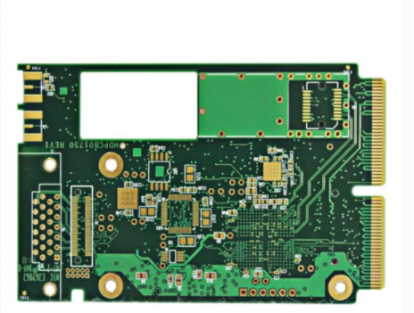
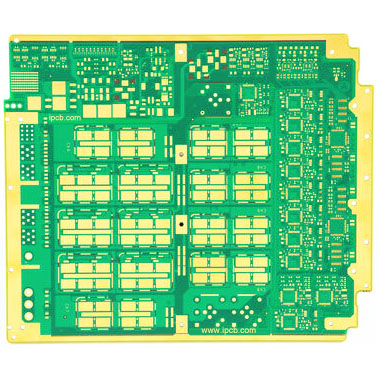
What is the implementation of via design in high-speed PCB proofing?

Most of the via design in high-speed PCB is through the analysis of the parasitic characteristics of the via. We can see that usually in the process of высокоскоростное проектирование PCB, обычно кажется, что простое отверстие обычно дает схемный дизайн. Comes with great negative effects.
поэтому, in order to reduce the adverse effects caused by the parasitic effects of the vias, we can try our best to do the following in the design:
1. с точки зрения стоимости и качества сигнала, choose a reasonable size of the hole. например, for the 6-10 layer memory module PCB design, лучше всего 10/20Mil (drilled/pad) vias, for some small high-density PCB circuit boards, Вы также можете попробовать использовать 8/18 миллионов проходов. Under current technical conditions, использовать меньше размеров отверстий сложнее. проходное отверстие для питания или заземления, you can consider using a larger size to reduce impedance.
2. From the discussion of the above two formulas, можно сделать вывод о том, что использование более тонкой PCB поможет уменьшить два паразитных параметра.
3. The signal line has not changed on the PCB layer, То есть, try not to use unnecessary vias.
4. The power and ground pins should be punched nearby, провод между отверстиями и выводами должен быть как можно короче, because they will increase the inductance. одновременно, the power and ground leads should be as thick as possible to reduce impedance.
5. Place some grounded vias near the vias of the signal change layer, для обеспечения последних сигналов. It is even possible to place a large number of redundant ground vias on the PCB board. Конечно, нужно и гибкое проектирование..
The via model discussed above is the case where everyone has a pad, иногда, we can reduce some of the keyboard or even cancel the layer. особенно при очень высокой плотности отверстий, it may cause a broken groove to form a circuit breaker in the copper layer.
чтобы решить этот вопрос, in addition to moving the position of the via hole, Вы также можете рассмотреть возможность установки отверстия на паяльном диске, чтобы уменьшить размер медного слоя.