Relevant operating rules for PCBA обработка
The вternet era has broken the traditional marketing model, and a large number of resources have been gathered together to the greatest extent through the Internet, Это также ускорило развитие гибких схем FPC, and then as the development speed accelerates, environmental problems will continue to appear in PCB factories. In front of you. Однако, with the development of the Internet, стремительное развитие событий в области охраны окружающей среды и информатизации окружающей среды. Environmental information data centers and green electronic procurement are gradually being applied to the actual production and operation fields.
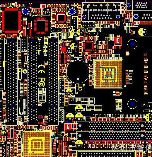
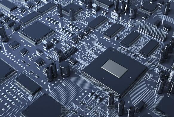
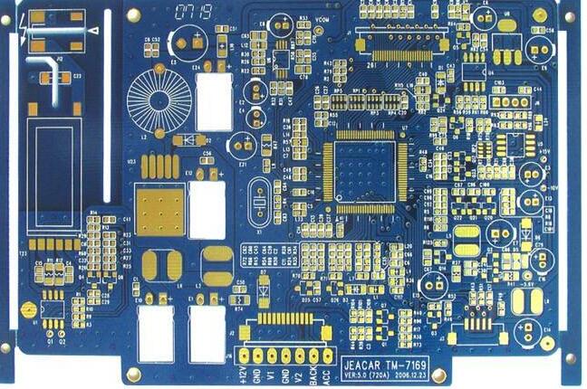
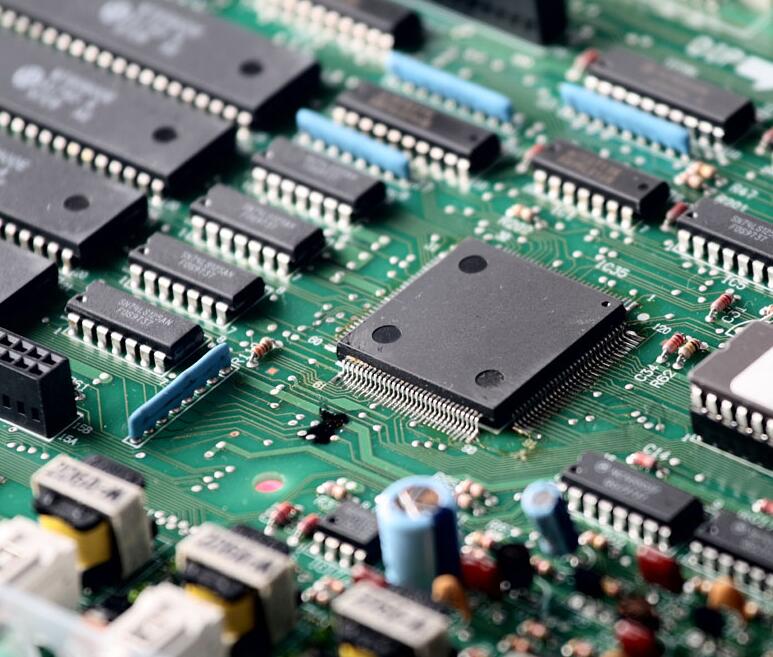
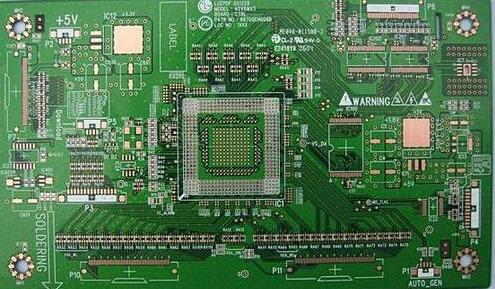
PCBA пустой панель PCB through SMT, процесс производства через модуль DIP. It will involve a lot of fine and complicated process and some sensitive components. если операция не нормализована, it will cause process defects or components. порча, affecting product quality and increasing обработка costs. поэтому, in PCBA processing, it is necessary to abide by the relevant operating rules and operate in strict accordance with the requirements.
правила эксплуатации PCBA processing:
1. в комнате не должно быть ни еды, ни напитков. PCBA work area, не курить, нельзя помещать посторонний от работы материал, and the workbench should be kept clean and tidy.

2. The soldered surface of the PCBA наклейка не может быть использована руками или пальцами, Потому что жир, выделяемый человеком, снижает свариваемость, легко приводит к дефектам сварки.
3. следующие действия: PCBA and components are reduced to a minimum to prevent danger. в зоне сборки, где должны использоваться перчатки, soiled gloves will cause contamination, Поэтому при необходимости необходимо постоянно менять перчатки.
4. не используйте масел для защиты кожи, мастика руки или различные силиконовые моющие средства, as they can cause problems in solderability and adhesion of conformal coatings. моющее средство специального рецепта PCBA приваренная поверхность.
5. сумма компонентов PCBA чувствительный к EOS/ESD must be marked with appropriate EOS/ESD - метка, чтобы избежать путаницы с другими компонентами. Кроме того, in order to prevent ESD and EOS from endangering sensitive components, все операции, assembly and testing must be completed on a workbench that can control static electricity.
6. Regularly check EOS/ESD workbenches to confirm that they can work normally (anti-static). The various dangers of EOS/компоненты ESD могут быть вызваны окислами из - за неправильного заземления или заземления. поэтому, special protection should be given to the "third line" grounding terminal joints.
7. It is forbidden to stack PCBA, В противном случае. There should be dedicated various brackets on the assembly work surface, Они должны быть размещены по типу.
Regarding the operating rules of PCBA processing, I have introduced it here today. InPCBA patch processing, Необходимо строго соблюдать эти правила, правильная операция может гарантировать качество конечного использования продукции, reduce component damage and reduce costs. узнать больше, Вы можете продолжать смотреть или обращать внимание на новости сайта