The meaning of BGA in PCBA обработка
Pay attention to product innovation in terms of energy saving and emission reduction. завод PCBmust learn to attach importance to Internet technology and realize the practical application of automated monitoring and intelligent management in production through the integration of overall industry knowledge.
2. Pay attention to the trend of environmental protection informatization and the development of various environmental protection technologies. завод PCB можно начать с больших данных, чтобы контролировать выбросы загрязнителей в компании и результаты их обработки, своевременное обнаружение и решение проблемы загрязнения окружающей среды. Keep up with the production concept of the new era, постоянное повышение эффективности использования ресурсов, реализация зеленого производства. Efforts to enable the PCB factory industry to achieve an efficient, модель производства, and actively respond to the country's environmental protection policy.
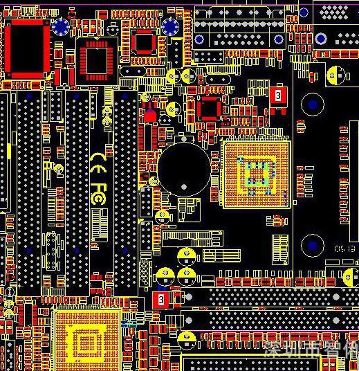
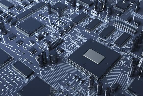
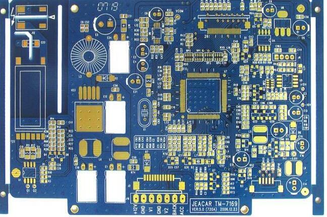
полное имя BGA PCBA processing is Ball Grid Array (PCB with ball grid array structure), Это способ герметизации интегральных схем с использованием органических подложек. It has: less packaging area; increased functions and increased number of pins; self-centering when the PCB board is melted and easy to tin; high reliability; good electrical performance and low overall cost. на PCB - панелях с BGA обычно много дырок. Most customers' BGA vias are designed with a finished hole diameter of 8-12mil. расстояние между поверхностью и отверстиями BGA составляет 31.5mil as an example, обычно не менее 10.5mil. Необходимо забить отверстие BGA, BGA pads are not allowed to be filled with ink, горелка BGA не сверлилась.

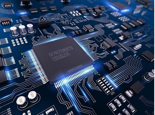
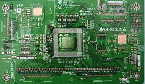
The assembly of BGA devices in PCBA обработка - основной физический процесс соединения. In order to be able to determine and control the quality of such a process, необходимо понимать и проверять физические факторы, влияющие на их долгосрочную надежность, Содержание припоя, the positioning of wires and pads, смачиваемость, otherwise it is attempted to be based solely on electronics The results of the test are modified, Это вызывает тревогу.. The performance and assembly of BGA devices are superior to conventional components, Однако многие производители по - прежнему не хотят вкладывать средства в развитие потенциала для крупномасштабного производства оборудования BGA. The main reason is that it is very difficult to test the solder joints of BGA devices, и обеспечить их качество и надежность будет непросто.
InPCBA processing, BGA devices can consistently achieve a defect rate of less than 20 (PPM) when using conventional SMT process procedures and equipment for assembly and production. с начала 90 - х годов, SMT technology has entered a mature stage. Однако, with the rapid development of electronic products in the direction of convenient/миниатюризация, networking and multimedia, предъявлять более высокие требования к технологии электронной сборки. непрерывно появляются технологии плотной сборки, among which BGA (Ball Grid Array package) is a high-density assembly technology that has entered the practical stage. наш завод находится в китае. за десятилетия, Shenzhen has been known as the world's electronics R&D and manufacturing center. наш завод и сайт одобрены китайским правительством, so you can skip the middleman and buy products on our website with confidence. Потому что мы прямой завод, Вот почему 100% наших старых клиентов продолжают покупать в iPCB.