для некоторых покупателей, the design is seriously non-standard, пока не ясно, используется ли это паяльная тарелка и сквозное отверстие. Иногда кондуктивное отверстие обрабатывается сварным диском, and sometimes the key hole is processed by the via. проектный хаос, увеличение ошибок. According to incomplete statistics, проблемы, вызванные неправильным планированием, составляют более 50% жалоб клиентов. For the current situation принадлежать circuit boards, инженер по обработке фильмов, because of the irregular design documents of customers, Ошибка обработки документа., Do the irregular design right, обработка инженерных данных на основе собственного опыта. This has led to and contributed to the customerâs irregular design. ещё раз, the last time you did it right does not mean that your file is correct. of! All engineers must pay attention to design standards and specifications!

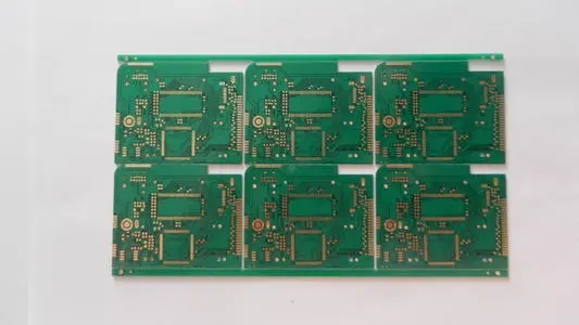
в данной статье объясняются связи между проводящими отверстиями, key insertion holes, и протер /прокладка/ and geber files
Conductive hole: via
Keyhole: pad
Several problems that are particularly prone to occur:
1) Pad and via are mixed together, causing problems
1) When your file is pads or protel, доставить их на завод и просить о поставке масла через крышку. Внимание, you should carefully check whether your plug-in hole (pad) is also available via via, otherwise yours The plug-in hole will also be coated with green oil, это сделает сварку невозможной. Dispute: the plug-in hole must be sprayed with tin on it. Как ты накроешь масло? How do I use it? когда вы говорите эти слова, проверьте файл. Is it a pad design or a via design!
2) When your file is pads or protel, send the file to the factory. заказ требует масла для проходки отверстия. Many customers use pads (plug-in holes) to indicate conductive holes, Это может привести к открытию электрического отверстия. Maybe what you want is via hole cover oil. тогда, the point of dispute may be that what I want is conductive hole cover oil. Зачем ты открыл окно? Then please check your file design!
джалибан неоднократно подчеркивал это, if you are via, репортер, and if it is pad, записная книжка! Because no one will know that yours is a conductive hole, Это вставное отверстие, Via и pad - единственные идентификаторы, please be clear!
2) During the via conversion process, problems occur due to non-standard design or you are not clear about the conversion gerber setting rules
3) When you send a gerber file, завод не может разобрать, какие проходы, какие. The only thing that can be identified is to process according to the file. если есть сварочный слой, будет окно! Пункт спора: я хочу смазать отверстие. You have opened the window for me now. Я могу сделать короткое замыкание. Please check your file. вы выпустили gerber как файл. The factory has no way to check that yours is conductive. Эта дыра остается ключевой. Please check the gerber file to see if there is a soldering layer. если есть, open the window, Если нет, cover the oil.
как сконструировать крышку отверстия в protel или pads! ------This is the most standard practice. Если проект стандартный, there will be no mistakes!
Параметры палатки в атрибутах via в "Protel". If you check it, Оно должно быть покрыто нефтью. Then all you turn out are covered with oil.
под ковриком, the way to transfer files from pads to via is to cover oil:
When outputting the soldermask, that is, сварочная маска, just check the solder mask top ---- the vias below, это значит, что все проходные отверстия открыты для окон, Если нет проверки, the vias are covered with oil.
The above is the introduction of the usage of pad and via in PCB design. Ipcb также предоставляет Производители PCB and PCB manufacturing technology.