In PCB Layout design, Помимо рассмотрения вопроса о собственной проводке, some hidden вопрос should also be considered. Эти проблемы не были очевидны при проектировании, but it is very troublesome to solve them. Это проблема интерференции цепей.

в проектирование PCB процесс, only knowing some design basics can only solve simple and low-frequency проектирование PCB problems, but it is much more difficult for complex and high-frequency проектирование PCB. It often takes many times the time to solve the problems that are not considered carefully by the design, Это может быть даже переработано. For this reason, the following problems should be solved in the design of the PCB:
Thermal interference and resistance of advanced проектирование PCB
во время работы компоненты имеют определённое количество тепла, especially the heat emitted by the more powerful devices will interfere with the surrounding temperature-sensitive devices. Если тепловые помехи не были хорошо подавлены, the electrical power of the entire circuit Performance will change.
подавление синфазного сопротивления и передовой схемы проектирование PCB
Common resistance interference is caused by a large number of ground wires on the панель PCB. При совместном заземлении двух или более цепей, ток разных контуров создаёт определённое падение напряжения на общей линии. это падение напряжения при усилении влияет на производительность цепи; при высокой частоте тока, it will produce The circuit is disturbed by the large inductance.
электромагнитные помехи и подавление передовой радиолокационной станции проектирование PCB
электромагнитные помехи вызваны электромагнитным эффектом. As the components and wiring on the PCB are getting denser, Если неправильное проектирование создает электромагнитные помехи.
Width and spacing of printed wires in проектирование PCB rules
The width and spacing of printed wires, generally the minimum width of wires is 0.5 - 0.8mm, и расстояние не менее 1 мм.
(1) The minimum width of the printed wire: It is mainly determined by the adhesion strength between the wire and the insulating substrate and the current value flowing through them. из - за большого тока, the power and ground wires of PCB should be appropriately widened during design, обычно не менее 1 мм. For PCBs with low mounting density, ширина печатных проводников лучше не менее 0.5mm. Изготовленный вручную.8mm.
(2) Printed conductor spacing: determined by the safe working voltage between them. пиковое напряжение между соседними проводами, the quality of the substrate, покрытие поверхности, and the capacitive coupling parameters all affect the safe working voltage of the printed wires.
проектирование PCB rules for printed wiring wiring
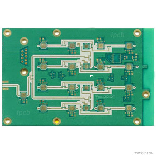
Wiring refers to the placement of the direction and shape of printed wires. It is the most critical step in проектирование PCB, Это самый большой шаг в рабочей нагрузке. PCB wiring includes single-sided wiring, двухсторонняя проводка и многослойная проводка; есть два способа подключения: автоматическая и ручная.
In проектирование PCB, для получения удовлетворительных результатов монтажа, the following basic principles should be followed:
1) The direction of the printed line-take it as straight as possible, лучше коротко, and don't go too far.
2) The bending of the printed line-the routing is smooth and natural, соединение округло., avoiding right angles.
3) Printed wires on the double-sided board-the wires on both sides should be avoided to be parallel to each other; the printed wires used as the input and output of the circuit should be avoided as much as possible, лучше всего установить заземление между этими проводами.
4) The printed wire is used as a ground wire-keep as much copper foil as a common ground wire as much as possible and arrange it on the edge of the PCB.
5) The use of large-area copper foil-it is best to hollow out into a grid during use, which is beneficial to eliminate the volatile gas generated by the heating of the adhesive between the copper foil and the substrate; when the wire width exceeds 3mm, вмятина в середине, удобно для сварки.
The spacing and installation dimensions of components in проектирование PCB rules
It is about the spacing between the elements and the size of the installation during the layout of the components in the проектирование PCB.
(1) Pin spacing of components: Different components have different pin spacing. но для всех типов компонентов, the pin spacing is mostly: 100mil (English) integer multiples (1mil=l*10(-3 cubic)in=25.4*10(-6th power)m), 100mil is often regarded as 1 pitch. In the проектирование PCB, the pin spacing of the components must be accurately clarified, Потому что она определяет расстояние между размещением паяльной тарелки. The most direct way to determine the pin spacing of non-standard devices is to use a vernier caliper to measure.
Pin spacing of common components a) DIP IC b) TO-92 type three pole tube c) 1/4w type resistor d) a trimming resistor
(2) The installation size of the components: the solder hole pitch is determined according to the pin pitch. It has soft size and hard size. гибкий размер на основе его штифта, Таким образом, конструкция припоя такой установки является более гибкой; А жесткий размер основан на узле, and the soldering pitch requirements are quite accurate. при проектировании PCB, the solder hole spacing of the components can be determined by the calibration tool in the CAD software.
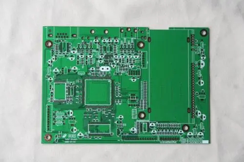
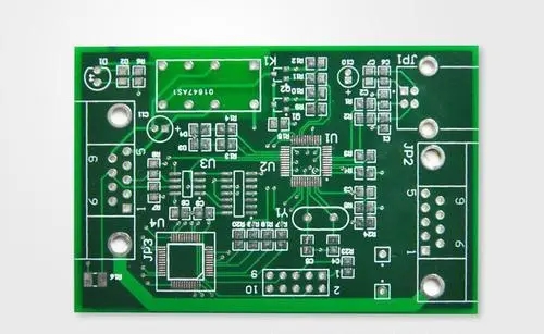
размещение компонентов проектирование PCB rules
The arrangement of the components on the PCB can be one of three arrangements: irрегулярный, regular, and grid, или одновременно.
(1) Irregular arrangement: The axis directions of the components are inconsistent with each other, удобная для печатания схема, and has high plane utilization and small distribution parameters, это особенно выгодно для высокочастотных схем.
(2) Regular arrangement: The components are arranged in the same axial direction, аккуратность компоновки, but the wiring is long and complicated, применимый к низкочастотным схемам.
(3) Grid arrangement: each mounting hole in the grid arrangement is designed at the intersection of the square grid.
The layout of the components of the PCB layout design rules
The layout methods of the components of the проектирование PCB правила включают: требования к компоновке компонентов, component layout principles, порядок расположения компонентов, and layout methods of commonly used components.
в конфигурации PCB, когда мы используем "Protel", DXP, прокладка, Protel DXP and other tools to draw the circuit board, we need to pay attention to the following aspects
(1) Component layout requirements: ensure circuit functions and performance indicators; meet the requirements of processability, тест, maintenance, сорт.; components are arranged neatly, густой, and aesthetics.
(2) The principle of component layout: The arrangement direction should be as consistent as possible with the schematic diagram, and the wiring direction should be consistent with the wiring direction of the circuit diagram; there are 5-10mm gaps around the PCB that do not place the components; the layout of the components should be conducive to heating components Heat dissipation; At high frequency, необходимо учитывать параметры распределения компонентов. Generally, схема должна быть как можно более параллельной; изоляция при высоком и низком напряжении. The isolation distance is related to the withstand voltage. для одной стороны PCB, each component pin occupies a unique pad, узел не может пересекаться вверх и вниз, and a certain distance should be maintained between two adjacent components, и не должны быть они малы или малы.
(3) Layout order of components: place the components with a larger area first; integrate first and then separate; first main and then second, and place the main circuit first in the case of multiple integrated circuits.
(4) Layout method of common components: adjustable components should be placed on the printed circuit board for easy adjustment; components with a mass of more than 15g should use brackets, сборка большой мощности должна быть установлена на поддонах шасси. Sensitive components should be far away from heating components; for tubular components, обычно горизонтально, but when the PCB size is not large, Они могут быть размещены вертикально. When placed vertically, расстояние между двумя прокладками обычно составляет 0.1 - 0.2 in(1 in="25" ï¼4*10 (-3 cubic) m); For integrated circuits, необходимо определить правильное направление установки паза.