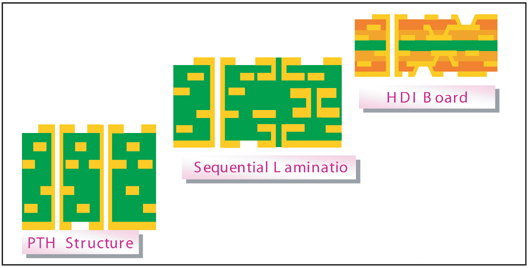
профиль схемы HDI
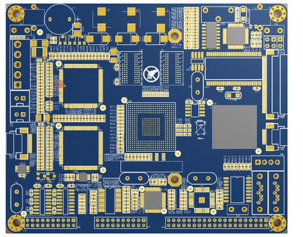
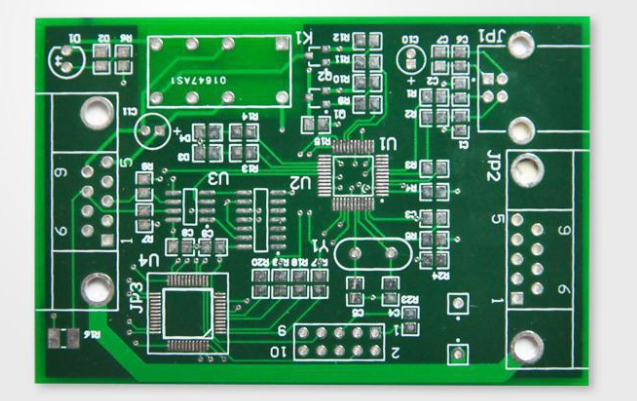
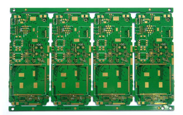
панель HDI (English is high-densityinterconnectboard) is a kind of circuit board with high wiring density in micro-blind via technology. этот панель HDI is divided into an inner layer circuit and an outer layer circuit, and the internal connection of each layer circuit board is realized through the method of drilling and metallization.
поэтому, the higher the application of HDI technology, Чем выше уровень изготовления слоистых плит. заурядный панель HDI is laminated once, использовать два типа HDI, три или более методом стратификации, Заполните отверстие гальваническим покрытием, гнездо сваи, прямая лазерная скважина.
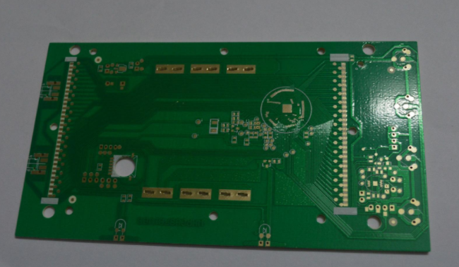
Are all blind and buried PCB circuit boards called HDI circuit boards?
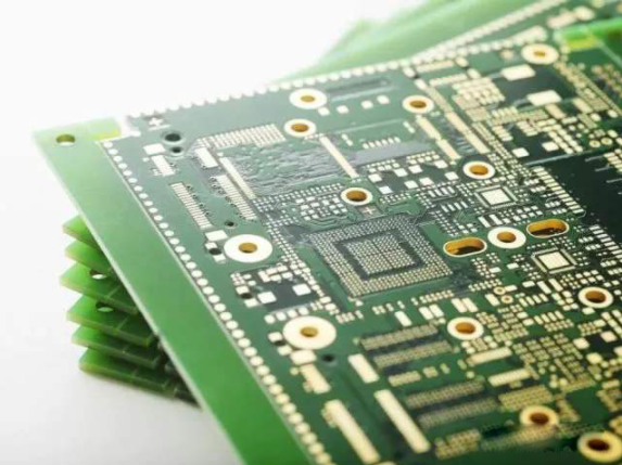
этот панель HDI is a high-density interconnect circuit board. после покрытия слепой дыры, the floor is панель HDI нажимать дважды. HDi boards are divided into 1, 2, 3, 4 и 5 панель HDIs. например, for mobile phones after iphone6, использовать основную панель 5 - го порядка HDI. так просто подземный переход is not necessarily an hdi circuit board.

как распознать первую, 2nd and 3rd order of the hdi circuit board
The easiest thing for everyone to understand is: Level 1 is the easiest to produce, с точки зрения параметров и технологий он относительно легко контролируется. Tier 2 and above are relatively difficult, особенно пятый этаж труднее всего контролировать.