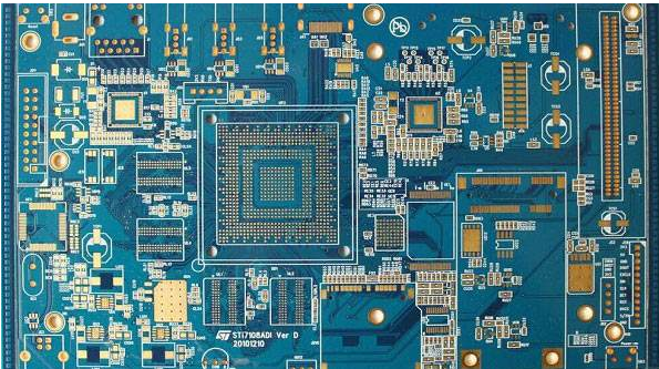
Analysis of common conditions of печатная плата welding
1. After soldering, на столе много грязных досок поверхность печатная плата:
1. It is not preheated before soldering or этот preheating temperature is too low (dip soldering, the time is too short).
2. этот board moves too fast (FLUX fails to evaporate sufficiently).
три. The temperature of the tin furnace is not enough.
4. It is caused by adding anti-oxidant or anti-oxidizing oil to the tin liquid.
5. Too much flux is applied.
6. The component foot and the board hole are out of proportion (the hole is too large) to increase the flux.
9. During the use of FLUX, долгое время не добавлять разбавитель.
Second, on fire:
1. The wave furnace itself does not have an air knife, Это может привести к чрезмерному потоку, which drips onto the heating tube during preheating.
2. The angle of the air knife is wrong (makes the flux coating uneven on the печатная плата).
три. There are too many adhesive strips on the печатная плата, Это зажигает ленту.
4. The board travel speed is too fast (FLUX is not completely volatilized, FLUX drips) or too slow (causing too high temperature on the surface of the board).
5. Process problem (панель печатная плата плохое расстояние между нагревательными трубами и подогревательными трубами печатная плата is too close).
три. Corrosion (components turn green, solder joints turn black)
1\\ Insufficient preheating (low preheating temperature, fast board moving speed), resulting in more FLUX residues and too many harmful residues).
2\\ Use the flux that needs to be cleaned, несвоевременная очистка или очистка после сварки.
Fourth, соединение питания, leakage (poor insulation) печатная плата неразумное проектирование, wiring is too close, сорт. печатная плата solder mask is of poor quality and easily conducts electricity.
5. Missing welding, виртуальная сварка, continuous welding The amount of FLUX coating is too small or uneven. Серьезное окисление на некоторых паяльных дисках или ногах. печатная плата wiring Это неразумно. (the distribution of components Это неразумно.). закупорка пенообразующей трубы, неоднородность пенообразования, Это приводит к неоднородности покрытия флюса на поверхности печатная плата. Improper operation method when immersing tin by hand. отклонение цепи неразумно. гребень волны.

Six, the solder joints are too bright or the solder joints are not bright
1. This problem can be solved by choosing bright type or extinction type FLUX);
2. The tin used is not good (for example, Содержание олова слишком низко, etc.).
Seven, short circuit 1) Tin liquid causes short circuit:
A. Continuous welding occurred but not detected.
B. The tin liquid has not reached the normal working temperature, между точками сварки есть мост "оловянная проволока".
C, между точками сварки есть мост.
D. непрерывная сварка, the bridge is erected.
2) печатная плата problems: such as: the печатная плата itself has a solder mask falling off and causing a short circuit
Eight, the smoke is big, the taste is big:
1. The problem with FLUX itself
A. смола: если использовать обычную смолу, the flue gas will be larger
B. растворитель: это означает, что запах или раздражающий запах растворителя, используемого в флюсе, может быть относительно большим. C. Activator: smoke and pungent odor
2. The exhaust system is not perfect
Nine, брызгать, tin beads:
1) Process
A, low preheating temperature (FLUX solvent is not completely volatilized)
B, the board speed is too fast to reach the preheating effect
C, плохо скошенная цепь, there are bubbles between the tin liquid and the печатная плата, and tin beads are generated after the bubbles burst
D, improper operation method when dipping the tin by hand
E, working environment is humid
2) The problem of PC B board
A, the board surface is wet, неполное подогревание, or moisture is generated
B. конструкция выхлопных отверстий автомобиля печатная плата is unreasonable, приводить газ печатная плата and the tin liquid. C. The design of the печатная плата is unreasonable, нога слишком плотна., causing gas trapping.
10. The soldering is not good and the solder joints are not full. двухволновой метод. Активный компонент флюса полностью испарился при прохождении олова. The board travel speed is too slow, Это приводит к завышению температуры подогрева. FLUX coating is uneven. подушка и ступня блока сильно окислены, вызывать недостаток олова, too little FLUX coating; failure to completely infiltrate the печатная плата подушка и ступня. The печатная плата design is unreasonable; the layout of the components on the печатная плата is unreasonable, affecting some parts Tin on components
11. пропотевание флюса. The selection of FLUX is not suitable for the foaming tube hole is too large or the foaming area of the foaming tank is too low. понижение давления в пенообразующей трубе. Uneven thinner added too much
12. пузырь слишком хороший. The air pressure is too high. область вспенивания слишком мала. Too much FLUX is added to the soldering tank. разбавитель вовремя не присоединился, which causes the FLUX concentration to be too high
13. цвет флюса немного непрозрачный. A few photosensitive additives are added to FLUX. Эта присадка красится при свете света., но не влияет на свариваемость флюса. 14.печатная плата срыв сварной маски, peels off or blisters 1. более 80% причин печатная плата технология изготовления. Too many times of tin passing during hot air leveling 2. повышенная температура Оловянного раствора или подогрева 3. Too many times during soldering 4. в процессе ручной пропитки олова, the печатная плата stays on the surface of the tin liquid for longer than the solder paste printing