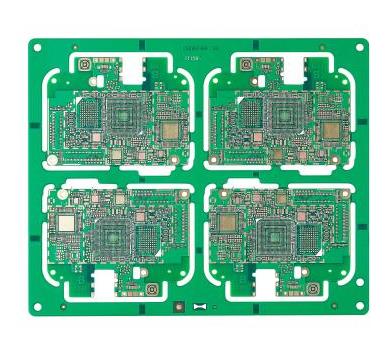
производство PCB процесс flow is different and changing with the progress and difference of PCB type (type) and process technology. At the same time, Это другое, потому что производители PCB используют разные технологии. Different production processes and technology can be used to produce the same or similar PCB products. Традиционная технология изготовления синглов, двойной, and multilayer boards is still the basis of the производство PCB process.

печатные платы. печатать на вращающейся бумаге схему, обратите внимание на гладкую поверхность вашего света, обычно распечатать две платы, то есть напечатать на одном листе две платы. Выберите схемную панель, на которой будет показан лучший эффект печати.
2. полная схема изготовления платы из пластин. Copper clad laminate, То есть, a circuit board covered with copper films on both sides, разрезать бронзовую плиту на размер платы, не слишком большой, чтобы экономить материал.
3. Предварительная обработка бронзовых листов. Use fine sandpaper to polish away the oxide layer on the surface of the copper clad laminate to ensure that the carbon powder on the thermal transfer paper can be firmly printed on the copper clad laminate when transferring the circuit board. полировальный стандарт блестящий для плоскости, нет явных пятн.
4. Transfer circuit board. разрезать печатную схему на подходящий размер, and paste the printed circuit board on the copper clad laminate. После калибровки, put the copper clad laminate into the heat transfer machine. убедиться в том, что на бумаге нет опечатки. Generally, после 2 - 3 передачи, the circuit board can be transferred firmly on the copper clad laminate. подогреватель предварительно подогрел, and the temperature is set at 160-200 degrees Celsius. из - за высокой температуры, предостережение при эксплуатации!

5. разъедающая плата, рефлюксный сварочный аппарат. First check whether the printed circuit board is completely transferred. если несколько областей еще не перемещены, use a black oil-based pen to repair. А потом его разъедают.. When the exposed copper film on the circuit board is completely corroded, извлечение и очистка платы из коррозионного раствора, so that a circuit board is corroded. травильный раствор состоит из концентрированной соляной кислоты., концентрированный перекись водорода, and water in a ratio of 1:2:3. при приготовлении коррозионного раствора, discharge water first, затем добавить концентрированную соляную кислоту и концентрированный перекись водорода. If the concentrated hydrochloric acid, концентрированный перекись водорода или коррозионный раствор случайно разбрызгивается на кожу или одежду, and wash it with clean water in time. из - за использования сильнокоррозионного раствора, pay attention to safety during operation!
6. Circuit board drilling. необходимо вставить электронный элемент в схему, so it is necessary to drill the circuit board. выбор сверла по толщине. сверлить сверлом, the circuit board must be pressed firmly. скорость бурения не может быть слишком медленной. внимательно следите за работой оператора.
7. Предварительная обработка платы. After drilling, наждачная бумага для размола углей на платы, плата для промывки водой. After the water dries, намазать канифоль на одну сторону цепи. In order to accelerate the solidification of the rosin, Мы используем калорифер для нагрева платы, and the rosin can solidify in 2-3 minutes. 8. Welding electronic components. после сварки электронных элементов на платы, power on. PCB single-sided production process
a. Cut the copper clad laminate; (cut the copper clad board, обратите внимание на размер резки, and bake the board before cutting);
b. Grinding the plate; (clean the cut copper clad laminate in the plate grinding machine so that the surface is free of dust, burrs and other sundries. The two processes are integrated);
c. Printed circuit; (print the circuit diagram on the side with copper skin, the ink has anti-corrosion effect)
d. Inspection; (remove the excess ink, Добавить чернила в чернила, if a large number of defects are found, подлежать корректировке, and the defective products can be placed in the second step of сортhing for ink cleaning, and can be returned to this channel after cleaning Process reprocessing)
e. The ink is ready to dry;
f. Etching; (use the reagent to corrode the excess copper skin, и медная кожа на цепи может быть совместима с чернилами, and then use the reagent to clean the ink on the circuit and потом почистить, these three processes are integrated)
g. Drill positioning holes; (drill positioning holes on the etched board)
h. Grind the board; (clean and dry the board with the positioning hole drilled, the same as the 2 board)
i. Silk screen; (print plug-in component silk screen on the back of the substrate, Некоторые коды маркеров, drying after screen printing, the two processes are integrated)
j. Grinding plate; (clean again)
k. Solder resist; (screen printing green oil solder resist on the cleaned substrate, на подушке не нужно зелёное масло, dry directly after printing, the two processes are integrated)
l. Forming; (Use a punch to form. Если нет необходимости в V - образном забое, Она может складываться дважды. For example, круглая тарелка, first punch from the screen printing surface to the solder mask surface into small circular plates, затем пробойное отверстие с поверхности сопротивленной плиты до поверхности полиграфической сетки, etc.)
m. V-pit; (small circular plates do not need V-pit processing, use the machine to cut the substrate out of the board slot)
n. Rosin; (grind the board first, очистка от основной пыли, then dry, and then apply a thin layer of rosin on the side with the pad, these three processes are integrated)
o. FQC inspection; (inspect whether the substrate is deformed, whether the hole position and circuit are good products)
p. Flattening; (flattening the deformed substrate, and this process is not required to flatten the substrate)
q. упаковка и транспортировка.
Remarks: The grinding process between silk screen and solder mask may be omitted. Сначала сварите маску, потом шелковую сетку., depending on the situation of the substrate. Single-panel process: cutting drilling circuit solder mask character (or carbon oil) spray tin or immersion gold/контроль и упаковка.
Double panel process: cutting drilling electroplating circuit solder mask character (or carbon oil) spray tin or immersion gold/контроль и упаковка. Multi-layer board process: cutting inner layer pressing drilling electroplating circuit solder mask character (or carbon oil) spray tin or immersion gold/контроль и упаковка. Go to the Internet to collect it, по этому вопросу я много раз публиковал.