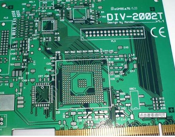
(1) The package of the components used on the PCB must be correct, включая размер и размер, шаг чеки, the number of the pins, размер и ориентация рамок, etc.
(2) The positive and negative poles or pin numbers of polar components (electrolytic capacitors, diodes, триод, etc.) should be marked in the PCB component library and on the панель PCB.
(3) The pin numbers of the components in the PCB library should be consistent with the pin numbers of the schematic components.
(4) For components that require heat sinks, the size of the heat sink should be taken into account when drawing the component package, Сборка и радиатор могут быть стянуты вместе, образуя целую форму упаковки.

(5) The inner diameter of the pin of the component and the pad should be matched, внутренний диаметр прокладки должен быть немного больше размера пальца узла, чтобы облегчить монтаж.
2. Requirements for PCB component layout
(1) The components are arranged uniformly, and the components of the same functional module should be arranged as close as possible.
(2) The components using the same type of power supply and ground network should be arranged together as much as possible, which is beneficial to complete the electrical connection between each other through the inner electrical layer.
(3) The interface components should be placed aside, and the interface type should be indicated with a character string, направление проводки обычно должно быть далеко от платы.
(4) Power conversion components (such as transformers, постоянный ток/DC converters, тройная регулирующая трубка, etc.) should have enough space for heat dissipation.
(5) The pins or reference points of the components should be placed on the grid point, Это способствует проводке и эстетике.
(6) The filter capacitor can be placed on the back of the chip, питание рядом с Чипом и заземляющий штырь.
(7) The first pin of the component or the sign indicating the direction should be marked on the панель PCB и не может быть покрыт компонент.
(8) The label of the component should be close to the component frame, равномерный по размеру, neat in direction, без перекрытия с паяльником и через отверстие, and cannot be placed in the area covered after the component is installed.