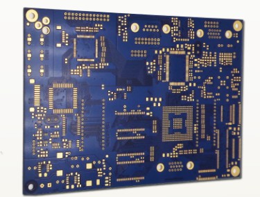
How to reduce the welding voids and defects of various IC chips on печатная платаA circuit boards
After the soldering of hardware печатная платаA electronic products is introduced into the lead-free process, из - за отсутствия свинца, высокая температура плавления, увлажняющая аберрация, narrow process window, сорт., the soldering process has unique defects and defects of lead-free soldering, сырьё и сварочная точка. Roughness, непровар, little tin, пустота.
It is well known that voids are formed when soldering large flat and low-foot height components, модуль QFN. The use of these types of components is increasing. для выполнения стандарта IPC, the formation of voids makes many плата печатная плата конструктор, печатная платаA soldering EMS foundries and quality control personnel feel a headache.
параметр оптимизации пустоты обычно химический состав масел, the температура орошения profile, покрытие базы и сборки, and the optimal design of the pad and the SMT stencil template. Однако, in practice, изменение этих параметров имеет явные ограничения. Несмотря на все усилия по оптимизации, но по - прежнему часто наблюдается высокий уровень вакансий.
The root cause of solder voids is that the air or volatile gas wrapped in the solder paste is not completely discharged after the solder paste is melted. факторы влияния включают оловянный материал, solder paste printing shape, рулон пасты, reflow temperature, reflow time, размер припоя, structure Wait.
тип техники: LGA, PGA, BGA

As an SMT engineer in the electronics manufacturing industry, if you do not master the SMT surface assembly process, трудно проанализировать и усовершенствовать этот процесс. До знакомства с процессом сборки, Вам нужно освоить конструкцию упаковки компонентов на поверхности. The package structure and assembly process are analyzed in detail.
IC chip and electronic components packaging structure
SMT surface mount component package type classification Surface mount component (SMD) package is the object of surface mount. понимание структуры упаковки SMD имеет важное значение для оптимизации процесса SMT. структура упаковки SMD является основой технологического проектирования. поэтому, here we are not classified by the name of the package but by the structure of the pin or the solder end. по этому сектору, SMD packages mainly include chip components (Chip), J - образный палец, L-shaped pin, BGA, BTC, и замок.
BGA package introduction:
1. BGA package (Ball Grid Array), according to its structure, mainly includes plastic package BGA (P-BGA), flip-chip BGA (F-BGA), carrier tape BGA (T-BGA) and ceramic BGA (C-BGA) ) Four categories.
широко используются устройства VTC для сварки нижней части платы, such as special devices such as ball array devices (BGA/поставщик услуг/WLP/POP) and QFN/LLP. The BTC package is listed in the BTC package listed in IPC-7093 There are QFN (Quad Flat No-Lead package), SON (SmallOutline No-Lead), DFN (Dual Flat No-Lead), LGA (land Grid Array), MLFP (Micro Leadframe Package).
среди, QFN is a leadless package, квадрат или. There is a large exposed pad at the center of нижний слой package for heat conduction, осуществлять электрическое соединение через обшивку. Потому что нет никаких зацепок, монтажная площадь меньше, and the height is lower than QFP. Плюс отличные электрические и тепловые свойства, this kind of package is increasingly used in the electronics industry.
управление зазором на диске радиатора QFN является одной из проблем при сварке QFN, Это одна из проблем отрасли..
As small-size packages are more capable of carrying high-power chips, пакет терминала (например, QFN) становится все более важным. As the requirements for reliability performance continue to increase, оптимизация тепловых и электрических свойств компонентов управления питанием в таких упаковках, как QFN. In addition, максимальное повышение скорости и радиочастотных характеристик, уменьшение пористости очень важно для уменьшения пути тока в цепи. As the package size shrinks and power requirements increase, рыночные требования уменьшают разрыв под тепловыми подушками компонентов QFN. Therefore, необходимо оценить ключевые технологические факторы, порождающие пробелы, и разработать оптимальные решения.
The QFN package has excellent thermal performance, в основном из - за большой площади теплоотводящей подушки на дне упаковки. In order to effectively conduct heat from the chip to the печатная плата, the bottom of the печатная плата must be designed with corresponding heat dissipation pads and heat dissipation vias. радиатор обеспечивает надежную сварную область, сквозное отверстие обеспечивает способ охлаждения. Therefore, когда открытый паяльный арочный на дне кристалла приваривается к горячей сварной тарелке на кристалле печатная плата, the gas in the solder paste on the thermal vias and the large-size pads will overflow, вызывать определенные поры. For the smt process In terms of large cavities, удалить эти поры практически невозможно. The only way to reduce the pores is to minimize them.
LGA - массив, or "planar grid array package", То есть, a package with array state electrode contacts made on the bottom surface. форма очень похожа на модуль BGA, because its land size is larger than that of BGA balls. диаметр примерно в 2 - 3 раза больше, and it is also difficult to control the voids. то же самое, что и компоненты QFN, промышленный стандарт еще не установлен, это в какой - то мере создает проблемы для электронной промышленности.
The full name of BGA is called "ball grid array", или "пакет сетки". сейчас, the vast majority of intel mobile CPUs use this packaging method, например, all intel processors ending in H, штаб, U, Y, сорт. ((включая, но не ограничиваясь, низкое напряжение)).
BGA can be the extreme product of LGA and PGA, это отличается от функции, которую можно свободно менять. Once the BGA is packaged, обычный игрок не может разобрать и заменить его обычным способом, but because it is done at one time., BGA может быть короче.
The main defects of BGA chip solder joints are: voids, desoldering (open circuit), bridging (short circuit), трещина внутри сварного шарика, solder joint disturbance, холодная сварка, incomplete solder ball melting, and displacement (the solder ball is not aligned with the печатная плата pad ), solder beads, etc.