There are many kinds of PCB production process flow charts. технология производства по ламинам платы и платам, it is divided into: double-sided circuit board process flow, технологический процесс с многослойной схемой, PCB copper electroplating process, технология обработки станков с цифровым управлением, PCB There are several main production processes for line pattern transfer and shape processing.
The basic manufacturing process of the factory to produce PCB circuit boards
Printed boards can be divided into single-sided, двухсторонняя и многослойная печатная плата зависит от числа слоёв проводника. The basic manufacturing process of a single panel is as follows:
Foil-clad board-->Unloading-->Baking board (to prevent deformation)-->Mould making-->Washing, drying-->Film (or screen printing) ->Exposure and development (or anti-corrosion ink)- ->Etching-->Film removal--->Electrical continuity inspection-->Cleaning treatment-->Screen printing solder mask pattern (printed with green oil)-->Curing-->Screen printing marking symbols-->Curing- ->Drilling-->Shape Processing-->Cleaning and Drying-->Inspection-->Packaging-->Finished Product.
The basic manufacturing process of double-sided panels is as follows:
In recent years, Типичным методом изготовления двухстороннего металлизированного печатного листа является метод SMOBC и гальваническое нанесение рисунков. В некоторых случаях, the process wire method is also used.

1. Graphic electroplating process
Foil Clad Laminate-->Cutting-->Punching and Drilling Benchmark Holes-->CNC Drilling-->Inspection-->Deburring-->Electroless Plating Thin Copper-->Plating Thin Copper-->Inspecting--> Brushing-->Filming (or screen printing)-->Exposure and developing (or curing)-->Inspection and repairing-->Pattern plating (Cn ten Sn/Pb)-->Removing film-->Etching- ->Inspect and repair the board-->Plug nickel-plated gold- ->Curing-->Shape Processing-->Cleaning and Drying-->Inspection-->Packaging-->Finished Product.
в процессе, the two processes of "electroless plating of thin copper --> electroplating of thin copper" can be replaced by a single process of "electroless plating of thick copper", у каждого из них есть свои плюсы и минусы. Pattern electroplating---etching method to make double-faced metallized plates is a typical process in the 1960s and 1970s. середина 80 - х, the bare copper-clad solder mask process (SMOBC) gradually developed, и стала основной технологией, особенно при точном двойном производстве панелей.
2. Bare Copper Clad Solder Mask (SMOBC) process
The main advantage of SMOBC board is that it solves the short-circuit phenomenon of solder bridging between thin lines. одновременно, из - за постоянного соотношения свинца и олова, it has better solderability and storage properties than hot melt board.
существует множество способов изготовления SMOBC, including the SMOBC process of standard pattern electroplating subtraction and lead-tin stripping; the subtractive pattern electroplating SMOBC process of using tin plating or immersion tin instead of electroplating of lead-tin; the plugging or masking hole SMOBC process ; Additive method SMOBC technology and so on. Ниже приводится описание схем гальванизации и отделки свинца и олова методом SMOBC и методом забивания..
процесс гальванизации рисунков SMOBC аналогичен методу гальванизации рисунков, прежде чем отделка свинца и олова. Changes only after etching.
Double-sided copper clad board-->According to the pattern electroplating process to the etching process-->Pb-Sn-->Inspection-->Cleaning--->Solder mask pattern-->Plug nickel plating and gold plating--> Adhesive tape for plugs-->Hot air leveling-->Cleaning--->Screen printing mark symbols--->Shape processing--->Cleaning and drying--->finished product inspection-->Packaging-->finished product.
PCB process
The film bottom plate is the leading process of printed circuit board production, качество тонкопленочных пластин непосредственно влияет на качество изготовления печатных плат. When producing a certain kind of printed circuit board, должна быть как минимум одна соответствующая пластинка. Each kind of conductive pattern (signal layer circuit pattern and ground, power layer pattern) and non-conductive pattern (solder mask pattern and character) of the printed board should have at least one film negative. процесс фотохимического перехода, various patterns are transferred to the production board.
The uses of film masters in printed circuit board production are as follows:
The photosensitive mask patterns in pattern transfer include circuit patterns and photoresist patterns.
изготовление сеток в процессе печати, рисунок и символ сварочного фотошаблона.
Machining (сверление and profile milling) CNC machine tool programming basis and drilling reference.
With the development of the electronics industry, растущие требования к печатным материалам. The high-density, тонкая нить, and small-aperture designs of printed boards tend to be faster and faster, Непрерывно совершенствуется технология изготовления печатных плат. In this case, Если нет мастера высококачественного кино, high-quality printed circuit boards can be produced. The production of modern printed boards requires the film master to meet the following conditions:
The dimensional accuracy of the film master must be consistent with the accuracy required by the printed board, and compensation should be made taking into account the deviation caused by the production process.
графика негатива должна соответствовать требованиям проектирования, Графические символы должны быть полными.
The edges of the graphics of the film master are straight and neat, край не выдуман; чёрно - белый контраст, which meets the requirements of the photosensitive process.
мембранная основа должна иметь хорошую стабильность размеров, that is, мелкомасштабные изменения, вызванные изменением температуры и влажности окружающей среды.
The film masters of double-sided and multi-layer boards require good overlap of pads and common patterns.
каждый слой в основной версии должен быть четко помечен или назван.
The film base can transmit the required wavelength of light, диапазон длины волны для материалов общей фоточувствительности 3000 - 4000а.
In the past, когда мастер кино, it was generally necessary to produce a photo master first, А потом с фотографией или пиратством. This year, с быстрым развитием компьютерной техники, the production process of film masters has also developed greatly. применение передовых технологий лазерного фотораспыления, что значительно повышает скорость производства и качество мастера, продукция высокой точности, thin-wire patterns that could not be completed in the past, making the CAM technology of printed board production tend to be perfect
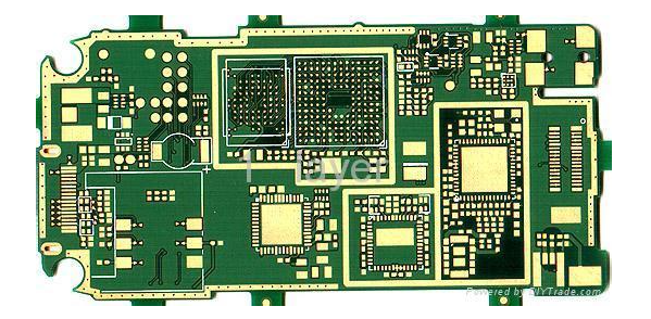
Copper Clad Laminates (Copper Clad Laminates, abbreviated as CCL), referred to as copper clad laminate or copper clad laminate, is the substrate material for manufacturing printed circuit boards (hereinafter referred to as PCB). At present, наиболее распространенным методом PCB, используемым при травлении, является Селективное травление на медных пластинах для получения рисунка требуемой схемы. The copper clad laminate is mainly responsible for the three functions of conduction, изоляция и поддержка на всей печатной схеме. The performance, качество и стоимость изготовления печатных плат в значительной степени зависят от бронзовых листов..
The main process flow of the plugging method is as follows:
Double-sided Foil Clad Laminate-->Drilling-->Chemical Copper Plating-->Plating Copper on the Whole Board-->Blocking Holes-->Screen Printing Imaging (Erect Image)-->Etching-->Removing Screen Printing, Remove plugging material-->Cleaning-->Solder mask pattern-->Plug nickel plating, gold plating-->Plug tape tape-->Hot air leveling-->The following procedures are the same as the above to the finished product.
Этапы этого процесса относительно просты, ключ в том, чтобы закрыть эти отверстия и очистить чернила, забитые ими.
In the hole plugging process, печать изображений в виде чернил и шелковой сетки, a special masking dry film is used to cover the hole, затем экспозиция, формирование позитивного образа, это процесс маскировки. Compared with the hole blocking method, У него больше нет проблем с чисткой чернил в отверстии, but it has higher requirements for masking the dry film.
технология SMOBC основана на первом производстве металлизированных пластин с голыми медными отверстиями, and then apply a hot air leveling process.
PCB engineering production
For the production of печатная плата, because many designers do not understand the production process of circuit boards, схема, которую они проектировали, была лишь основной схемой, которая не могла быть непосредственно использована для производства.. Therefore, перед реальным производством необходимо изменить и изменить файл схемы. Not only need to make a film chart suitable for the factory's production process, но также необходимы данные о штамповке, mold opening data, и другие полезные для производства данные. It is directly related to various future production projects. все это требует от инженеров и техников знания необходимых производственных процессов и производства соответствующего программного обеспечения, включает в себя общее программное обеспечение для проектирования схем, например, "Protel", Pads2000, Autocad, etc., и ознакомление с необходимым программным обеспечением CAM, таким как View2001, CAM350; GCCAM And so on, CAM должен включать ввод PCB, which can edit, правильно, repair and imposition circuit graphics, использовать диск как средство, and output automated data for light drawing, drilling, and testing.