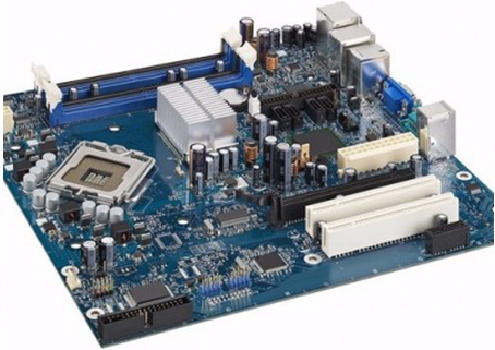
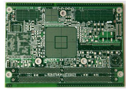
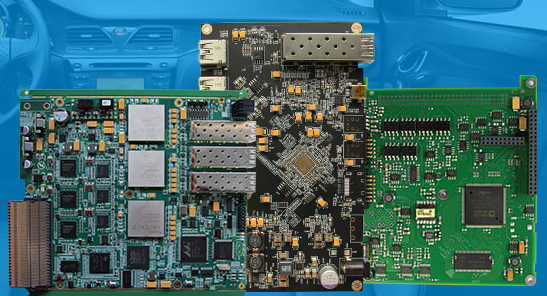
[First trick] Multi-layer board wiring High-frequency circuits tend to have high integration and high wiring density. использование многослойных плат не только необходимо для проводки, but also an effective means to reduce interference.
этап размещения PCB, a reasonable selection of the printed board size with a certain number of layers can make full use of the intermediate layer to set up the shield, лучше всего добиться ближайшего приземления, and effectively reduce the parasitic inductance and shorten the signal transmission length, Все эти методы повышают надежность высокочастотных схем, such as reducing signal cross-interference.
Некоторые данные показываются при использовании одного и того же материала, the noise of the four-layer board is 20dB lower than that of the double-sided board.
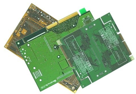
Однако, there is also a problem. Чем выше количество слоя PCB, the more complicated the manufacturing process and the higher the unit cost. Это требует от нас не только выбора подходящего уровня, но и выбора соответствующего уровня PCB. рациональная компоновка компонентов, and use correct wiring rules to complete the design.
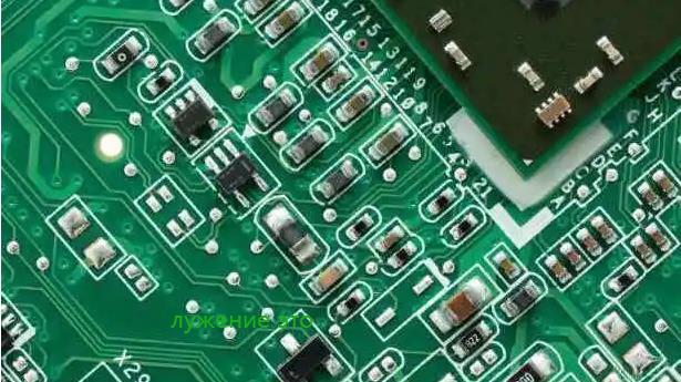
[Second trick] The lead between the pins of high-speed electronic devices should be bent as little as possible. проводка высокочастотной цепи лучше всего использовать полную прямую, which needs to be turned. Он может вращаться по ломаной или дуге 45 градусов. только для повышения прочности медной фольги, but in high-frequency circuits, выполнение этого требования может уменьшить внешние эмиссии высокочастотных сигналов и взаимную связь.
[Third trick] The shorter the lead between the pins of the high-frequency circuit device, лучше. The radiation intensity of the signal is proportional to the length of the signal line. длина хода высокочастотного сигнала, чем легче будет сочетаться. высокочастотная сигнальная линия, crystal oscillator, данные DDR, LVDS line, USB - линия, HDMI line, сорт., it is required to keep the trace as short as possible.
[Fourth measure] The less the lead-layer alternation between the pins of the high-frequency circuit device, лучше. The so-called "the less the lead-layer alternation, лучше" refers to the fewer vias (via) used in the component connection process, the better . On the data side, один проход может принести 0.5pF of distributed capacitance. уменьшение количества отверстий может значительно повысить скорость и уменьшить вероятность ошибок в данных.
[Fifth trick] Pay attention to the "crosstalk" introduced by signal lines in close parallel routing. High-frequency circuit wiring should pay attention to the "crosstalk" introduced by signal lines in close parallel routing. последовательный сигнал - линия без прямого соединения. Coupling phenomenon.
Потому что высокочастотные сигналы передаются по линиям передачи в форме электромагнитных волн, сигнальная линия будет служить антенной, энергия электромагнитного поля будет излучаться вокруг линии передачи. Undesired noise signals are generated due to the mutual coupling of electromagnetic fields between the signals. Called crosstalk (Crosstalk).
The parameters of the PCB layer, расстояние между сигнальными линиями, электрические характеристики привода и принимающего конца, and the signal line termination method all have a certain impact on the crosstalk.
поэтому, in order to reduce the crosstalk of high-frequency signals, При подключении следует, насколько это возможно, сделать следующее:, Вставка заземления или заземления между двумя проводами, более сильно пересекающимися. снятие помех.
When there is a time-varying electromagnetic field in the space surrounding the signal line, если невозможно избежать параллельного распределения, a large area of ground can be arranged on the opposite side of the parallel signal line to greatly reduce interference.
Если поле подключения разрешено, increase the spacing between adjacent signal lines, уменьшить параллельную длину линии сигнала, and try to make the clock line perpendicular to the key signal line instead of parallel. Если параллельные следы в одном и том же слое почти неизбежны, в двух соседних слоях направление линии должно быть перпендикулярно.
в цифровых схемах, the usual clock signals are signals with fast edge changes, высокий внешний шум. поэтому, в проекте, it is advisable to surround the clock line with a ground wire and punch more ground wire holes to reduce distributed capacitance, Таким образом уменьшать соучастие. For the high-frequency signal clock, Попробуйте использовать низковольтный разностный часовой сигнал и заземленный режим, and pay attention to the integrity of the ground hole.
неиспользованный входной зажим не должен висеть, but grounded or connected to the power supply (the power supply is also grounded in the high-frequency signal loop), Потому что линия подвески может быть равносильна передающей антенне, заземление подавляет передачу. Practice has proved that using this method to eliminate crosstalk can sometimes yield immediate results.
[Sixth trick] Add a high-frequency decoupling capacitor to the power supply pin of the integrated circuit block. Add a high-frequency decoupling capacitor to the power supply pin of each integrated circuit block. увеличение емкости высокочастотной развязки на штырях питания эффективно подавляет помехи от высокочастотных гармоник на педали питания.
[Seventh trick] The ground wire of high-frequency digital signal and the ground wire of analog signal should be isolated. при соединении с имитацией заземления, цифровое заземление, etc. общий заземление, use high-frequency choke magnetic beads to connect or directly isolate and choose a suitable place Single point interconnection.
потенциал земли по высокочастотным цифровым сигналам обычно не совпадает, and there is often a certain voltage difference between the two directly. и, the ground wire of the high-frequency digital signal often contains very rich harmonic components of the high-frequency signal. при прямом соединении заземления цифровых сигналов с линией аналоговых сигналов, the harmonics of the high frequency signal will interfere with the analog signal through the ground wire coupling.
Therefore, under normal circumstances, заземление высокочастотных цифровых сигналов и аналоговых сигналов должно быть отделено, можно использовать одноточечное или высокочастотное дроссельное соединение.
[Eighth Tip] Avoid loops formed by traces. Try not to form loops in various high-frequency signal traces. Если неизбежно, make the loop area as small as possible.
[Ninth trick] It is necessary to ensure good signal impedance matching. в процессе передачи сигналов, when the impedance does not match, сигнал будет отражен в канале передачи. The reflection will cause the synthesized signal to form an overshoot, вызывать колебание сигнала вблизи логического порога.
The fundamental way to eliminate reflection is to match the impedance of the transmission signal well. Чем больше разница между сопротивлением нагрузки и сопротивлением линии передачи, Чем больше отражение, so the characteristic impedance of the signal transmission line should be made equal to the load impedance as much as possible.
одновременно, note that the transmission line on the PCB must not have sudden changes or corners, максимально сохранять сопротивление в каждой точке линии передачи, В противном случае будет отражаться между отрезками линии передачи.
This requires that during high-speed PCB wiring, необходимо соблюдать следующие правила подключения:.
Requires USB signal differential routing, ширина линии 10 мм, line spacing 6mil, расстояние между заземленными и сигнальными линиями 6 мил.
HDMI wiring rules.
Нужна разность сигналов HDMI, the line width is 10mil, Шаг 6 mil, and the spacing between each two sets of HDMI differential signal pairs exceeds 20mil.
правила электропроводки LDS.
Requires LVDS signal differential routing, ширина линии 7 мм, line spacing 6mil, the purpose is to control the differential signal pair impedance of HDMI to 100+-15% ohm DDR wiring rules.
установочная линия DDR1 требует сигнала не пропускать отверстие. The signal lines are of equal width and the distance between lines. проводка должна соответствовать принципу 2W, чтобы уменьшить помехи между сигналами. For high-speed devices of DDR2 and above, данные высокой частоты. The lines are equal in length to ensure the impedance matching of the signal.
[Tenth trick] Maintain the integrity of signal transmission. Maintain the integrity of signal transmission and prevent the "ground bounce phenomenon" caused by ground wire splitting.