How does PCB control impedance?
непрерывно повышается скорость переключения сигналов PCB, today's PCB planning manufacturers need to understand and control the impedance of PCB traces. в современных цифровых схемах относительно короткое время передачи сигнала и более высокая частота часов, линия PCB больше не простая, but transmission lines.
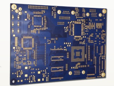
фактически, it is necessary to manipulate the trace impedance when the digital edge speed is higher than 1ns or the analog frequency exceeds 300Mhz. One of the key parameters of a PCB trace is its characteristic impedance (То есть, the ratio of voltage to current when the wave is transmitted along the signal transmission line). характеристическое сопротивление проводника на печатных платах является важным показателем планирования платы, especially in the PCB planning of high-frequency circuits, необходимо рассмотреть вопрос о том, являются ли характерные импеданцы проводников одинаковыми и соответствуют ли они характеристикам, оборудованию или сигналу. . Речь идет о двух понятиях: Управление сопротивлением и согласование импедансов. основное внимание в настоящем документе уделяется вопросам импедансов и планирования стека.

Impedance control
Impedance control (eImpedance Controling), проводник в платы будет передавать различные сигналы. In order to increase its transmission rate, Необходимо увеличить его частоту. Changes in impedance will result in distortion of the signal. поэтому, the impedance value of the conductor on the high-speed circuit board should be controlled within a certain range, Это называется "импедансное управление".
The impedance of the PCB trace will be confirmed by its inductive and capacitive inductance, сопротивление и проводимость. Основными факторами, влияющими на сопротивление линии PCB, являются ширина медной линии, the thickness of the copper wire, диэлектрическая постоянная среды, толщина среды, the thickness of the pad, путь к заземлению, и провода вокруг. The range of PCB impedance is 25 to 120 ohms.
фактически, the PCB transmission line is generally composed of a wire trace, один или более опорных и изоляционных материалов. The trace and the board layer constitute the control impedance. PCB обычно выбирает многослойную структуру, and the control impedance can also be constructed in various ways. Однако, no matter what method is used, the impedance value will be determined by its physical structure and the electrical characteristics of the insulating material:
The width and thickness of the signal trace
The height of the core or pre-filled material on both sides of the trace
Trace and layer configuration
Insulation constant of core and pre-filled material
There are two main forms of PCB transmission lines: Microstrip and Stripline.
Microstrip:
A microstrip line is a ribbon wire, which refers to a transmission line with a reference plane on only one side. The top and sides are exposed to the air (coating layer can also be applied), and it is located on the surface of the insulation constant Er circuit board. питание или уровень земли как ссылки. As shown below:
Note: In practical PCB manufacturing, завод планшетов обычно окрашивает слой зеленого масла на поверхности PCB. Therefore, в реальном импедансе, the model shown in the figure below is generally used for the calculation of the surface microstrip line:
Stripline:
Strip line is a strip wire placed between two reference planes. Как показано на диаграмме ниже, the dielectric constants of the dielectrics represented by H1 and H2 can be different.
Два приведенных примера - типичная демонстрация миниатюрных и полосатых линий. Конкретные микрополоски и полосы имеют много видов, such as coated microstrip lines, Это специфическое слоистая плита PCB structure.
формула для расчета сопротивления свойства требует сложных математических вычислений. В общем, the field solution method is used, включая анализ элементов зазора. Therefore, использование специального импеданса для вычисления SI9000, what we need to do is to control the parameters of the characteristic impedance:
The dielectric constant Er of the insulating layer, the wiring width W1, W2 (trapezoid), the wiring thickness T and the insulating layer thickness H.
Explanation on W1 and W2:
The calculated value must be within the red box. Другие условия можно вывести из сравнения классов.
The following uses SI9000 to calculate whether the impedance control requirements are met:
First, calculate the single-ended impedance control of the DDR data line:
TOP layer: the copper thickness is 0.5OZ, ширина траектории 5 мм, the distance from the reference plane is 3.8 миль, диэлектрическая постоянная 4.2. Select the model, параметр замены, выбор неразрушающих вычислений, as shown in the figure:
Coating indicates the coating layer. Если нет покрытия, fill 0 in thickness and 1 (air) in dielectric (dielectric constant).
подложка, подложка, То есть, the dielectric layer, Общие параметры FR - 4, the thickness is calculated by impedance calculation software, and the dielectric constant is 4.2 (when the frequency is less than 1GHz).
Click on the Weight(oz) item, Вы можете установить толщину бронзовой плиты, and the copper thickness determines the thickness of the trace.
9. The concept of Prepreg/Core of the insulating layer:
PP (prepreg) is a kind of dielectric material, из стекловолокна и эпоксидной смолы. Core is actually a PP type medium, но обе его стороны покрыты медной фольгой, while PP does not. при изготовлении многослойных листов, как правило, CORE и PP используются совместно, CORE and CORE are bonded with PP.
10. Matters needing attention in PCB stack-up planning:
(1), warpage problem
The слоистая плита PCB plan should be symmetrical, that is, the dielectric thickness of each layer and the copper thickness are symmetrical. взять в пример шестислойный, the dielectric thickness and copper thickness of TOP-GND and BOTTOM-POWER are the same, GND - L2 имеет ту же толщину диэлектрика и меди, что и L3 - POWER. такой, no warpage occurs during lamination.
(2) The signal layer should be tightly coupled with the nearby reference plane (that is, the dielectric thickness between the signal layer and the nearby copper layer should be small); the power copper and ground copper should be tightly coupled.
(3) Under very high-speed conditions, можно соединить избыточные пласты, чтобы перекрыть сигнальный слой, but it is recommended not to block multiple power layers, Это может вызвать ненужные шумовые помехи.
(