The line drawn by TopLayer (top layer) is red, which is the upper layer of a general double-sided board, and this layer is not used for a single-sided board.
The line drawn by BottomLayer (bottom layer) is blue, which is the line layer above the single panel.
MidLayer1 (MidLayer1) This is the first middle layer. It seems to have 30 layers. В общем, designers can't use it. Тебе не о чем беспокоиться.. It is used when there are multiple panels. значение по умолчанию не указано в 99SE, and it is not used.
Mechanical Layers (purple red) are used to mark the size and the board description, игнорировать в процессе тестирования копия PCB processing, То есть, the board is invisible when it is made, Это означает простое замечание.
Top Overlay (the top silk screen layer) (yellow) is the characters on the front of the board. This layer of characters can be used for the TopLayer (top layer) single panel. The Bottom Overlay (bottom screen layer) (brown) corresponds to the BottomLayer (bottom layer), Какой совет директоров. For the characters on the back, использовать оба уровня при печати.
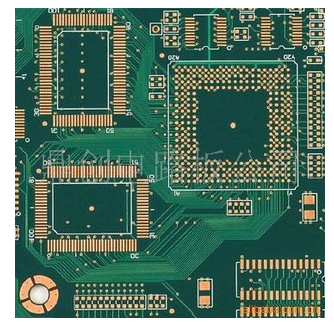
KeepOutLayer (prohibited wiring layer) (purple red with the mechanical layer) is simply the frame and appearance of the board.
Multi layer (multi-layer) (silver) All wiring layers are included. В общем, односторонняя и двухсторонняя прокладка на этом этаже, все слои рисуются полосками..
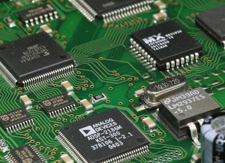
1. TopLayer (top layer) The top layer wiring layer, used to draw electrical connections between components.
2. BottomLayer (bottom layer) bottom wiring layer, Он служит проводкой верхнего слоя.
3.MidLayer1 (MidLayer1) is used to draw electrical connection lines on this layer when making multilayer boards, но высокая стоимость многослойных плит.
4. Mechanical Layers (mechanical layers) формат печатной доски PCB, and the parts that need to be dug, также можно пометить размер PCB, etc., can be used to draw the shape of the PCB printed board, and the parts that need to be dug, не использовать один и тот же механический слой для создания PCB, cutouts and PCB annotation dimensions. например, mechanical layer 1 is used to draw the PCB shape and cutouts, механический слой 13. After separation, технические работники изготовителя печатных плат будут следить за содержанием этого слоя и самостоятельно анализировать его, с тем чтобы определить необходимость его изготовления.
5. Top Overlay (the top silk screen layer) (yellow) is the characters on the front of the board. This layer of characters can be used for the TopLayer (top layer) single panel. Bottom Overlay (the bottom silk screen layer) (brown) corresponds to BottomLayer (bottom layer). это персонаж с обратной стороны доски. использовать оба уровня при печати.

6. KeepOutLayer (forbidden wiring layer) is used to draw the prohibited wiring area. If there is no mechanical layer drawn on the printed board, Производители печатных плат будут рассматривать этот слой как PCB. если одновременно использовать запрещенный слой и механический слой, По умолчанию используется mechanical слоёв как форма PCB, but the technicians of the printed board manufacturer will distinguish it by themselves, Но если они не могут различать, they will default to the mechanical layer. слой формы.
7. Multi layer (multi-layer) (silver) All wiring layers are included. Generally, single and double-sided plug-in pads are on this layer, and the stripes are drawn on all layers.
О, Signal Layers (signal layer)
Protel98 and Protel99 provide 16 signal layers: Top (top), Bottom (bottom) and Mid1-Mid14 (14 middle layers).
сигнальный слой служит проводником для завершения проволоки из медной фольги для печатных плат. When designing a double-sided board, generally only two layers of Top (top) and Bottom (bottom) are used. When the number of printed circuit boards exceeds 4 layers, Mid (middle wiring layer) is required.
Two, Internal Planes (internal power supply / ground plane)
Protel98 and Protel99 provide Plane1-Plane4 (4 internal power/ground planes). The internal power/приемные пласты используются главным образом для печатных плат более 4 этажей, как специальный слой электропитания и заземления, и не надо использовать двухсторонний лист.
три, Mechanical Layers (mechanical layer)
The mechanical layer is generally used to draw the frame (boundary) of the printed circuit board, обычно используется только один механический слой. There are Mech1-Mech4 (4 mechanical layers).
4, Drkll Layers (drilling position layer)
has 2 layers: "Drill Drawing" and "Drill Guide". диаметр и расположение отверстий.
5, Solder Mask (solder mask)
has 2 layers: Top (top layer) and Bottom (bottom layer). создавать сварочный шаблон на защитной зоне вокруг паяльного диска и проходного отверстия на печатных схемах.
6, Paste Mask (Solder Paste Protective Layer)
has 2 layers: Top (top layer) and Bottom (bottom layer). The solder paste protective layer is mainly used for printed circuit boards with surface-mounted components. сейчас, it is required for the installation process of surface-mounted components, не требуется этот слой, если сборка не установлена на поверхности.
7, Silkscreen (silk screen layer)
has 2 layers: Top (top layer) and Bottom (bottom layer). The silk screen layer is mainly used to draw text descriptions and graphic descriptions, очертание, labels and parameters of components.
8, Other (other layers)