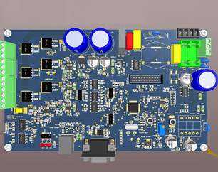
печатная плата schematic component design
If there are required components in the PROTEL component Партия освобожденияrary, Вы можете найти их и положить их на схему. If there is no required component, you need to create a new principle component library (Sch.lib). процесс: в исходном файле библиотеки компонентов, find the component 1 with the same (or similar) number of pins as the required component. When the cursor becomes a cross cursor, Переместить курсор на детали, click the mouse to determine a reference point. затем переключиться на Sch.lib Документация to be edited, and create a new device (shortcut creat component) in the file and modify it Name. SCH Lib щелчок в правом нижнем углу среды, move the mouse cursor to the empty component name, Щелчок правой кнопкой мыши, and execute in the pop-up shortcut menu
Paste command, Вставить компонент 1 в недавно созданную библиотеку компонентов. Then modify the pin properties. затем выполнить меню команды Report|составная часть Rule Check to perform the regulatory inspection.

2. печатная плата schematic design
Create a new печатная плата schematic file-->load the component library (including loading the component library you created)-->place the component-->the schematic wiring output device report<--correct the error--comile all projects<-set the compilation error first Report option (Reports/Bills of Materials) output network report (еслиre is no hierarchical schematic diagram, Вы можете создать только один документ/NetlistForDocument/протр, if there is a hierarchical module diagram, you need to generate a project network report (Protel) In the schematic design, if the схема is more complicated, you can use the hierarchical schematic design from top to bottom (or bottom to top).
3. Component печатная плата packaging design
You can use a component of the same (or similar) package to perform simple attribute modification to obtain the required component package. процесс копирования и изменения пакетов компонентов .pcbdoc to .печатная платаlib. No longer here. подробно изложить. No registration required
After the component package is modified, исполнительное редактирование/Set Preference/Вставка 1: установить точку отсчета упаковки в первом гнезде. Then execute Report/Проверка правил сборки, настройка всех правил, and OK. сейчас, the package is established.
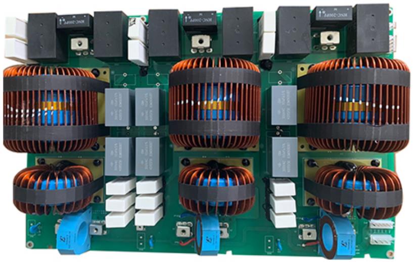
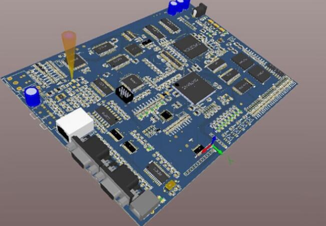
4. проектирование печатная плата
First create a new печатная плата file, & Импортировать таблицу сети после загрузки пакетов.
Automatic component layout. до этого шага, you must first set the size of the печатная плата, Вы должны планировать для него хороший размер и форму. Click on the bottom to select keep-out layer, затем в меню положение, select Draw Line, Нарисовать прямоугольник на черной подложке. You can choose the size.
Примечание: в данный момент нарисованная линия является розовой! This shows that you are planning the size of the circuit board in the keep-out layer. & Автоматическое размещение, routing can proceed smoothly.
какое бы программное обеспечение ни использовалось, there is a general procedure for проектирование печатная плата, Это сэкономит время и энергию, Поэтому я буду знакомить вас по производственным процессам..
Schematic design is the preliminary work. рисовать сразу начинающему панель печатная плата in order to save trouble. Это не вознаградит. For simple boards, если вы знакомы с процессом, you can skip it. но для начала, you must follow the process, Поэтому с одной стороны, you can develop good habits, С другой стороны, the only way to avoid mistakes for complex circuits.
при составлении схем, pay attention to the final connection of each file into a whole when designing the hierarchy, Это также важно для будущей работы. Due to differences in software, some software may appear to be connected but not connected (in terms of electrical performance). если не использовать соответствующие инструменты тестирования, in case something goes wrong, Теперь уже поздно узнать, когда будет готов Совет директоров.. Therefore, неоднократно подчеркивалась важность последовательной работы, and I hope to attract everyone's attention.
Проект, основанный на принципе, as long as the electrical connection is correct, нечего сказать.