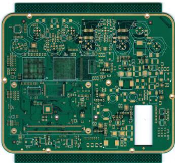
PCB companies commonly used circuit board processing processes are as follows: Single-panel process, двухпанельный способ, multi-layer board process, выбор материала PCB, PCB material selection a) The substrate with higher Tg should be selected appropriately-glass transition temperature Tg is a characteristic property of polymers, критическая температура, определяющая свойства материала, and a key parameter for selecting substrates. на основе эпоксидной смолы Tg около 125 - 140°C, and the reflow soldering temperature is around 220 degree Celsius, это гораздо выше, чем Tg на базовой панели PCB. высокая температура легко приводит к тепловой деформации PCB, при серьезном повреждении компонентов. *Tg should be higher than the working temperature of the circuit. b) Low CTE is required-due to the inconsistency of the thermal expansion coefficients in the X, направление по Y и толщине, it is easy to cause деформация печатной платы, в серьезных случаях, металлизированные отверстия разрываются, части ломаются. c) High heat resistance is required-generally the PCB is required to have a heat resistance of 250°C/более 50 лет. d) Good flatness is required. e) Electrical performance requirements: materials with low dielectric constant and low dielectric loss are required for high-frequency circuits. сопротивление изоляции, withstand voltage strength, стойкость к дуге должна соответствовать требованиям продукции.

PCB thickness design 1. допустимый толщина плиты обычных дисков: 0.5~5mm. 2. толщина PCB обычно 0.5~2mm. 3. Assemble only low-power components such as integrated circuits, маломощный транзистор, resistors, конденсатор, etc., при отсутствии вибрации под нагрузкой, use a thickness of 1.6 мм, and the size of the board within 500mm*500mm; 4. Да, при вибрации нагрузки, в зависимости от вибрации необходимо уменьшить размер платы или укрепить и увеличить опорную точку, и 1.6mm plate can still be used; 5. когда поверхность листа большая или не может быть удержана, consider increasing the plate thickness. надо выбрать доску толщиной 2 ~ 3мм. 6. когда Уровень выше, the thickness of each layer must be ensured to meet other requirements (such as withstand voltage requirements). 7. When the PCB size is smaller than the minimum mounting size, необходимо пользоваться посадочным способом. Design of laminated structure In the design of laminated structure, Мы привержены проектированию и производству слоистой структуры, отвечающей потребностям заказчика. Основные принципы проектирования заключаются в следующем:, Необходимо проектировать по требованию клиента. когда клиент имеет полное сопротивление, a laminate structure that meets the customer's requirements must be used. когда клиент не указывает структуру, the design principle is: the thickness of the dielectric layer and the pressing thickness meet the customer's requirements. Приоритет выбора толстых слоёв; минимальная диэлектрическая толщина: 0.06mm, по мере возможности, use a single PP structure. поверхностный ПП может разрядить только 1080 раз, 2116 laminate structure design software. требования к толщине среды были описаны в документе PCB серии Protel, что привело к неправильному пониманию структуры слоистой плиты, Как показано на правой диаграмме, if the layer is obtained without special settings The pressure structure is equal to the medium. затем толщина пластины уменьшена, the quantity of PP increases, и стоимость возросла. If there is no requirement, Предложение подробно описано в. Inner graphic design Inner graphic design The distance between the inner hole and the line should be increased as much as possible, более высокий, the greater the distance. (4 layer boards are guaranteed to be more than 7mil, 6-8 layers are guaranteed to be more than 8mil) более высокий, расстояние между внутренними отверстиями и медью, общий более 10 мл, which improves the reliability. в районах с плотной дыркой, трубопровод должен располагаться, насколько это возможно, между двумя отверстиями. The elements in the board are more than 15 mils away from the edge of the board. The higher the level, you can consider increasing it. нанести медь под золотыми пальцами, чтобы не допустить ухудшения области. Frequently Asked Questions-The inner network is not clear. A) The hole is tangent to the inner graph, and the network cannot be judged. B) The hole design is on the isolation line, and the PAD design of the hole location is incomplete, Невозможно определить сеть. C) The quincunx pad is designed on the isolated line, его сеть также не может быть установлена. Drilling design Drilling design 4) Thickness-to-diameter ratio: The ratio of hole to plate thickness is preferred: less than 1:8, когда 1: 8 или выше, трудно справиться. 5) When using the reflow soldering process, открыть окно как. В общем, the via hole diameter is not less than 0.3mm; отношение наименьшего отверстия к толщине пластины не менее 1: 8. если масштаб слишком мал, процесс усложняется, когда отверстие металлизируется. Rising costs. B. The via hole cannot be directly set on the pad, удлинительная часть прокладки и угол прокладки. C. между проходным отверстием и паяльной тарелкой должна быть тонкая линия, покрытая сварной маской. длина тонких линий должна быть больше 0.5mm and the width greater than 0.1 мм. Drilling design 6) The minimum hole diameter is 0.2 мм. Large holes can be used as much as possible. расстояние между кромкой отверстия и кромкой отверстия более 12 мм, and the via hole should not be drilled on the pad that needs to be soldered. 7) PCB aperture tolerance control range: The normal aperture tolerance is in accordance with the IPC 2 standard. допуск на диаметр прессованного отверстия может регулироваться ±0.05 мм. PTH can control the hole diameter tolerance ±0.08 мм. NTPH может регулировать допуск на отверстия ±0.05mm. 8) Hole position tolerance ±0.075mm 9) Hole copper requirements: IPC 3 standard control Hole copper average 25um, одна точка больше 20um. The most common problems of drilling files communicate the design of the outer circuit 1. ограничение шага 3/3MIL, минимальная ширина линии в готовом виде% 1OZ/spacing 4.5/4.5 мл, finished product 2OZ minimum line width/Шаг 6/6MIL, затем увеличить толщину меди до 1OZ, и ширина линии и расстояние соответственно увеличены на 1 мм, corresponding to the copper thickness of the inner layer line width and spacing. в зависимости от обстоятельств предлагается добавить 1 мил. 2. The current-carrying capacity of the line width at different temperatures (1OZ). внешний дизайн схемы 3. слезинка должна быть добавлена траектория траэтория паяного диска PCB to avoid the pad being pulled off during wave soldering. 4. No vias can be placed on the SMD pads, проходное отверстие и паяльная тарелка должны содержать 0.2m away.