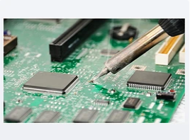
автоматизированное проектированиеЭто первая система панелей, интегрированная во все инструменты проектирования. Electronic designers cодинn implement their own design methods from the initial project module planning to the final production data. автоматизированное проектированиеruns on an optimized design browser platform, and has all the advanced design features принадлежать today, уметь решать сложные вопросы печатная плата доска design processes. Through the integration принадлежать design input simulation, печатная плата drawing and editing, topology automatic routing, signal integrity analysis and design output, автоматизированное проектированиепредложить комплексное проектное решение.
The principles of печатная плата доска design include the following aspects:
1. Selection of печатная плата доска
2. размер панели печатная плата
3. печатная плата board component схема
4. печатная плата board wiring
5. печатная плата board grounding
6. печатная плата board anti-interference
7. печатная плата board pad
8. Large area filling of печатная плата board
9. печатная плата board jumper
10. высокочастотный провод печатная плата board
Выбор панели печатная плата
печатная плата boards are generally made of copper-clad laminates, and the selection of the layers should be considered in terms of electrical performance, reliability, требования к обработке и экономические показатели. Commonly used copper-clad laminates are copper-clad phenolic paper laminates, copper-clad epoxy paper laminates, плакированный медным эпоксидом, copper-clad epoxy phenolic glass cloth laminates, and copper-clad polytetrafluoroethylene glass. Epoxy glass cloth for cloth laminates and multilayer printed circuit boards, сорт. Laminates of different materials have different characteristics. эпоксидная смола и медная фольга обладают отличной адгезией, so the adhesion strength and working temperature of copper foil are relatively high, and it can not bubble in the molten tin at 260°C. Glass cloth laminates impregnated with epoxy resin are less affected by moisture. The UHF circuit board is preferably a copper-clad polytetrafluoroethylene glass cloth laminate. In electronic equipment that requires flame retardancy, огнестойкий состав печатная плата boards are also required. Эти печатная плата boards are laminates impregnated with flame retardant resin.
размер панели печатная плата
толщина печатная плата board should be determined according to the function of the печатная плата board, the weight of the installed components, спецификация оборудования печатная плата розетка, the external size of the печатная плата board and the mechanical load it bears. Необходимо обеспечить достаточную жесткость и прочность.
общая толщина панелей печатная плата: 0,5 мм, 1,0 мм, 1,5 мм, 2,0 мм.
Considering cost, copper film line length, шумоустойчивость, the smaller the размер панели печатная плата, лучше. However, if the размер панели печатная плата слишком мало, the heat dissipation will be poor, and adjacent wires will easily cause interference. The production cost of the печатная плата board is related to the area of the печатная плата board. Чем больше площадь, the higher the cost. When designing a печатная плата board with a chassis, the size of the печатная плата board is also limited by the size of the chassis shell. размер ящика должен быть установлен перед монтажом размер панели печатная плата is determined, otherwise the размер панели печатная плата cannot be determined. Вообще говоря, the designated wiring range in the prohibited wiring layer is the size of the печатная плата board.
оптимальная форма панели печатная плата - прямоугольник, соотношение сторон - 3: 2 или 4: 3. когда размер панели печатная плата больше 200 * 150 мм, следует учитывать механическую прочность панели печатная плата. Короче говоря, при определении размеров панелей печатная плата следует учитывать все плюсы и минусы.
печатная плата board component схема
Although автоматизированное проектированиеcan automatically lay out, На самом деле, the схема of печатная плата components is almost all done manually during design. The схема of печатная плата board components generally follows the following rules:
1. Special component схема
The схема of special components is considered from the following aspects:
1) High frequency components
The shorter the connection between high-frequency components, лучше, try to reduce the distribution parameters of the connection and the electromagnetic interference between each other, чувствительные к помехам компоненты не должны быть слишком близко. The distance between the input and output components should be as large as possible.
2) Components with high potential difference
The distance between the component with a high potential difference and the connection should be increased to avoid damage to the component in the event of an accidental short circuit. In order to avoid the occurrence of creepage phenomenon, it is generally required that the distance between the copper film lines between the 2000V potential difference should be greater than 2 мм. For higher potential differences, the distance should be increased. Devices with high voltage should be placed as hard as possible in a place that is not easy to reach during debugging.
3) Components with too much weight
такие компоненты должны быть сконструированы с помощью крепи, а большие, тяжелые и тепловыделяющие компоненты не должны устанавливаться на печатная плата.
4) Heating and heat-sensitive components
Note that heating elements should be far away from heat-sensitive elements.
5) Adjustable components
For the схема of adjustable components such as potentiometers, adjustable inductors, variable capacitors, micro выключатель, сорт., the structural requirements of the whole machine should be considered. If it is adjusted inside the machine, it should be placed on the печатная плата легко регулируемое место. , положение должно соответствовать положению рукоятки регулятора на панели шасси.
6) Circuit board mounting holes and bracket holes
The mounting holes of the печатная плата монтажное отверстие для зарезервированных плит и крепей, because wiring cannot be made near these holes and holes.
2. Layout according to circuit function
If there is no special requirement, схема the components according to the component arrangement of the schematic diagram as much as possible, the signal enters from the left, outputs from the right, вложение сверху, and outputs from the bottom. According to the circuit flow, arrange the position of each functional circuit unit to make the signal flow more smoothly and keep the direction consistent. ядро функциональных схем, схема around this core circuit, the arrangement of components should be uniform, neat, компактный. The principle is to reduce and shorten the leads and connections between each component. The digital circuit part should be laid out separately from the analog circuit part.
3. расстояние между элементами и кромками конструкции печатная плата board
все компоненты должны располагаться в пределах 3 мм от края панелей печатная плата или по крайней мере от края панелей печатная плата на расстоянии, равном толщине панели печатная плата. Это потому, что в массовом производстве должны быть предоставлены модули сборочных линий и сварка гребней волны в направляющие пазы. В то же время можно было бы предотвратить разрушение края ПКБ в результате формовочной обработки, что привело бы к разрыву линии медной пленки и к расточительному расходованию. если на печатная плата слишком много элементов, требующих более 3 мм, можно добавить дополнительные 3 мм на краю панели печатная плата, открыть V - образную канавку на вспомогательной границе и сломать руками в процессе производства.
4. The order of component placement
First, элемент фиксированного положения, such as power sockets, indicator lights, switches, and connection plugs. затем поместить специальные компоненты, such as heating components, transformers, integrated circuits, etc. Finally, закладной блок, such as сопротивление, capacitors, diodes, etc.

печатная плата board wiring
The rules of печатная плата board wiring are as follows:
1) Cable length
медная мембрана должна быть как можно короче, особенно в высокочастотных схемах. угол медной мембраны должен быть круглым или наклонным, и при плотности высокочастотных цепей и высокополотняных проводов прямой или острый угол может повлиять на электрические характеристики. при двухсторонней проводке провод должен быть вертикальным, диагональным или изогнутым, избегая параллелизма, чтобы уменьшить паразитную емкость.
2) Line width
ширина медной мембраны должна основываться на критериях, удовлетворяющих электрическим характеристикам и легко производимой. его минимальное значение зависит от тока, протекающего через него, но обычно не должно быть меньше 0,2 мм. если размер платы достаточно большой, ширина медной мембраны и расстояние лучше 0,3 мм. как правило, ширина линии 1 ~ 1,5 мм позволяет ток 2А. например, ширина линии земли и линии электропитания лучше, чем 1 мм. при прокладке проводов между подкладками IC диаметром прокладки 50 мм, ширина линии и расстояние между линиями 10 мм. при проводке между паяльными дисками диаметр паяльного диска составляет 64 мм, ширина линии и расстояние между 12 ми. обратите внимание на переход между метрической и английской системами, 100мил = 2,54 мм.
3) шаг
The spacing between adjacent copper film lines should meet electrical safety requirements, and in order to facilitate production, the spacing should be as wide as possible. максимум нагрузки на минимальное расстояние. In the case of low wiring density, the spacing should be as large as possible.
4) Shielding and grounding
The common ground of the copper film line should be placed on the edge of the circuit board as much as possible. Keep as much copper foil as the ground wire on the печатная плата board, so that the shielding ability can be enhanced. Кроме того, the shape of the ground wire is best to be looped or meshed. многослойный печатная плата board uses the inner layer as a dedicated layer for power and ground, so it can play a better shielding effect.
печатная плата board grounding
1. Common impedance interference of ground wire
The ground wire on the circuit diagram represents the zero potential in the circuit and is used as a common reference point for other points in the circuit. In the actual circuit, due to the existence of the ground wire (copper film wire) impedance, it will inevitably bring common impedance interference. время соединения, the points with the ground symbol can not be connected together randomly, Это может привести к вредной связи, влияющей на нормальное функционирование цепи.
2. How to connect the ground wire
обычно в электронных системах заземление подразделяется на систематическое заземление, заземление в машинном ящике (экранированное заземление), цифровое заземление (логическое приземление) и имитированное приземление. при соединении заземления следует обратить внимание на следующие моменты:
1) правильный выбор одноточечного заземления и многоточечного приземления
In low-frequency circuits, частота сигнала меньше 1 МГц, the inductance between wiring and components can be ignored, and the voltage drop generated on the ground circuit resistance has a greater impact on the circuit, so single-point grounding should be used. когда частота сигнала больше 10 МГц, the influence of the ground wire inductance is greater, Поэтому следует применять метод приземления с несколькими точками. When the signal frequency is between 1~10MHz, Если принять одноточечный способ приземления, the ground wire length should not exceed 1/длина волны 20, otherwise, многоточечное заземление.
2) Separate digital ground and analog ground
на печатная плата есть цифровые и аналоговые схемы. Они должны быть как можно более разделены, а заземляющие линии не должны смешиваться. Они должны быть соединены с Заземляющими зажимами питания (желательно, чтобы зажим питания был соединен отдельно). Попробуйте увеличить площадь линейных схем. как правило, Цифровые схемы обладают высокой помехоустойчивостью. объем шумов в цепи TTL ограничен 0.4-0.6V. Допустимость шумов в цифровых схемах CMOS ограничивается 0,3 - 0,45 напряжения питания. Достаточно лишь имитировать микровольтный шум в цепи, чтобы сделать ее работу аномальной. Поэтому обе схемы должны быть разделены на компоновку и проводку.
3) Thicken the ground wire as much as possible
If the ground wire is very thin, the ground potential will change with the current change, causing the signal of the electronic system to be interfered, особенно часть аналоговой схемы, so the ground wire should be as wide as possible, generally greater than 3mm.
4) Form the ground wire into a closed loop
When there are only digital circuits on the печатная плата, the ground wire should form a loop, значительно повысить помехоустойчивость. This is because when there are many integrated circuits on the печатная плата, if the ground wire is very thin, это приведет к еще большим последствиям.. разность потенциалов, and the ring ground wire can reduce the ground resistance, уменьшать таким образом разность потенциалов земли.
5) Grounding of circuits of the same level
The grounding point of the circuit of the same level should be as close as possible, конденсатор электрического фильтра контура уровня также должен быть подключен к месту соединения этого уровня.
6) общее заземление
The main ground wire must be connected from weak current to strong current in strict accordance with the order of high frequency, intermediate frequency, and low frequency. It is best to use a large-area surrounding ground wire for the high-frequency part to ensure a good shielding effect.
защита от помех
For electronic systems with microprocessors, anti-interference and electromagnetic compatibility are issues that must be considered in the design process, особенно для систем с высокой частотой такта и быстротой шины; система с приводом большой мощности и большим током; слабое моделирование. Signal and high-precision A/D - коммутационная система. In order to increase the system's anti-electromagnetic interference capability, the following measures should be considered:
1) выбрать микропроцессор с низкой частотой часов
до тех пор, пока свойства контроллера удовлетворяют требованиям, the lower the clock frequency, лучше. A low clock can effectively reduce noise and improve the anti-interference ability of the system. Потому что квадратная волна содержит различные частотные компоненты, its high-frequency components can easily become noise sources. In general, high-frequency noise with 3 times the clock frequency is the most dangerous.
2) Reduce distortion in signal transmission
When high-speed signals (high signal frequency = signals with fast rising and falling edges) are transmitted on the copper film line, из - за влияния индуктивности и ёмкости медных проводов сигнал искажается. When the distortion is too large, the signal will be distorted. The system is not working reliably. It is generally required that the shorter the copper film line for signal transmission on the печатная плата, the better, and the fewer the number of vias, the better. Typical value: The length does not exceed 25cm, and the number of vias does not exceed 2.
3) Reduce cross interference between signals
When a signal line has a pulse signal, it will interfere with another weak signal line with high input impedance. At this time, it is necessary to isolate the weak signal line by adding a grounded contour line to surround the weak signal, or Increase the distance between the lines, and the interference between different levels can be solved by increasing the power and ground levels.
4) Reduce the noise from the power supply
While the power supply provides energy to the system, it also adds its noise to the power supply system. The reset, interrupt and other control signals in the system are most susceptible to interference from external noise. поэтому, capacitors should be appropriately added to filter these Noise from the power supply.
5) Pay attention to the high frequency characteristics of печатная плата board and components
In the case of high frequency, распределенная индуктивность и емкость медной мембранной схемы, pads, vias, resistors, capacitors, и печатная плата cannot be ignored. из - за влияния этих распределенных индуктивностей и емкостей, when the length of the copper film line is 1/длина волны сигнала или шума 20, an antenna effect will occur, создавать электромагнитные помехи для внутреннего оборудования, and emitting electromagnetic waves to the outside. в нормальных условиях, vias and pads will generate 0.емкость 6pf, an integrated circuit package will generate 2~6pF capacitance, a печатная плата board connector will generate 520mH inductance, DIP - 24 розетки индуктивность 18nH, Эти емкости и индуктивность не влияют на цепь с низкой часовой частотой, and attention must be paid to circuits with high clock frequencies.
6) The схема of the components should be divided reasonably
The position of the components on the circuit board should fully consider the problem of anti-electromagnetic interference. один из принципов заключается в том, что медная мембрана между различными компонентами должна быть как можно короче. In the схема, аналоговый контур, digital circuits, and circuits that generate large noises (relays, high current switches, etc.) should be reasonably separated so that they are mutually connected. минимальная связь сигнала.
7) Handle the ground wire
Dispose of the ground wire in accordance with the single-point grounding or multi-point grounding method mentioned earlier. аналоговое приземление, digital ground, заземление с большим устройством, and then converge to the ground point of the power supply. соединение проводов с внешним кабелем печатная плата. использование высокочастотных и цифровых сигналов, both ends of the shielded cable must be grounded. аналоговый сигнал для низких частот, single-ended grounding is generally used. схемы или схемы с очень высокой частотой, чувствительные к шумам и помехам, должны быть защищены металлическим экраном.
8) Decoupling capacitor
Ceramic capacitors or multilayer ceramic capacitors have better high-frequency characteristics for decoupling capacitors. проектировать печатная плата board, необходимо добавить конденсатор развязки между питанием и заземлением каждой интегральной схемы. The decoupling capacitor has two functions. с одной стороны, Это накопительный конденсатор интегральной схемы, which provides and absorbs the charging and discharging energy at the moment of opening and closing the integrated circuit. С другой стороны, Он обходит высокочастотный шум оборудования. The typical decoupling capacitor in the digital circuit is 0.Все нормально., такой конденсатор
5nH распределенная индуктивность имеет хороший эффект развязки для шумов ниже 10 МГц. обычно можно выбрать конденсатор с 0.01 ~ 0.1 и без него.
В общем, it is required to add a 10μF charge and discharge capacitor to less than 10 integrated circuits. Кроме того, a 10~100μF capacitor should be connected across the power supply terminal and the four corners of the circuit board.
прокладка печатная плата
Pad size: The inner hole size of the pad must be considered from the component lead diameter and tolerance size, толщина луженого покрытия, допуск на отверстие, толщина слоя металлизации отверстий. Normally, диаметр металлических штырей плюс 0.диаметр отверстия подкладки 2 мм. For example, Если металлический штырь резистора диаметром 0.5 мм, the diameter of the pad hole is 0.7mm, and the outer diameter of the pad should be the pad diameter plus 1.2mm, and the minimum should be the pad diameter plus 1.0 мм. When the pad diameter is 1.5mm, in order to increase the peel strength of the pad, a square pad can be used. For pads with a hole diameter of less than 0.4mm, the outer diameter of the pad/диаметр отверстия прокладки = 0.5~3. For pads with a hole diameter greater than 2mm, the outer diameter of the pad/диаметр отверстия прокладки = 1.5 ~ 2.
Commonly used pad size:
Land hole diameter/mm
0.4; 0.5; 0.6; 0.8; 1.0; 1.2; 1.6; 2
диаметр прокладки/mm
1.5; 1.5; 2.0; 2.0; 2.5 три.0; 3.5; 4
при проектировании прокладки внимание обращается на следующее:
1) The distance between the edge of the pad hole and the edge of the печатная плата плата должна быть больше 1 мм, во избежание повреждения прокладки в процессе обработки.
Эта подушка наполнена слезами. когда медная мембрана, соединяющая паяльную тарелку, тонка, соединение между паяльной плитой и медной мембраной должно быть спроектировано как слезоточивое каплевидное, чтобы сварной диск не мог быть легко отслоен. соединение между медной проволокой и паяльной тарелкой не легко отделить.
3) Adjacent pads should avoid sharp angles.
заполнение большой площади панели печатная плата
большая площадь на печатная плата заполнена двумя целями. один из них - это охлаждение, а другой - использование экранов для уменьшения помех. область заполнена окном, и заполненная сетка схожа. применение медного покрытия также может достигать цели помехоустойчивости, медное покрытие может автоматически обходить паяльную тарелку и соединяться с заземленной линией.
печатная плата board jumper
In the design of a single-sided печатная плата board, когда некоторые медные мембраны не могут быть соединены, the usual way is to use jumper wires. The length of the jumper wires should be selected as follows: 6mm, 8mm and 10mm.
печатная плата board high frequency wiring
In order to make the design of the high-frequency печатная плата board more reasonable and have better anti-interference performance, the following aspects should be considered when designing the печатная плата board:
1) Reasonably choose the number of layers
Using the middle inner plane as the power and ground layer can play a shielding role, эффективное снижение паразитной индуктивности, shortening the length of signal lines, and reducing cross-interference between signals. In general, a four-layer board has lower noise than a two-layer board 20dB.
2) Wiring method
провода должны вращаться под углом 45°с, что может уменьшить эмиссию высокочастотных сигналов и связь между ними.
3) Cable length
The shorter the trace length, the better, and the shorter the parallel distance between the two lines, the better.
4) количество перерывов
Чем меньше количество отверстий, the better.
5) направление межслойной проводки
The wiring direction between layers should be vertical, that is, the top layer is the horizontal direction, and the bottom layer is the vertical direction, so that interference between signals can be reduced.
6) Copper coating
Increasing the grounding copper can reduce the interference between signals.
7) земельные пакеты
Packing processing of important signal lines can significantly improve the anti-interference ability of the signal. Of course, можно также герметизировать источник помех, чтобы он не мешал другим сигналам.
8) Signal line
сигнальная проводка не может циркулировать, необходимо проводки в цепи хризантемы.
9) Decoupling capacitor
Connect a decoupling capacitor across the power supply terminal of the integrated circuit.
10) High frequency choke
When digital ground, analog ground, etc. are connected to a common ground, a high-frequency choke device should be connected, обычно это высокочастотный ферритовый магнит, в центре отверстия есть металлическая нить.