With the increase of PCB circuit board DK, it is more and more difficult to control the phase consistency of printed circuit board (PCB) materials. Accurately predicting phase changes of circuit board materials is not a simple or routine task. The signal phase of high frequency and high-speed PCB depends largely on the structure of the transmission line processed by it and the dielectric constant (DK) of the circuit board material. The lower the Dk of the medium (for example, the Dk of air is about 1.0), the faster the electromagnetic wave propagates. With the increase of Dk, the propagation of waves will slow down, and this phenomenon will also affect the phase response of the propagating signal. When the Dk of the propagation medium changes, изменение фазы формы колебаний, because a lower or higher Dk will make the speed of the signal in the propagation medium correspondingly faster or slower.
PCB circuit DK of material is usually anisotropic, with different Dk values in three dimensions (3D) of length, width, and thickness (corresponding to x, Y, and Z axes). For some special types of circuit design, it is necessary to consider not only the difference of Dk but also the impact of circuit manufacturing on phase. Phase stability and predictability will become increasingly important as PCB operating frequencies increase, especially at частота микроволн и миллиметровых волн, such as fifth-generation (5G) cellular wireless communication network infrastructure equipment, and advanced driver assistance systems (ADAS) in electronically assisted vehicles.

So what causes the Dk of circuit board material to change? In some cases, differences in The Dk on the PCB are caused by the material itself (e.g. changes in copper surface roughness). в других случаях, PCB - производство processes can also cause DK changes. In addition, a harsh working environment (such as high working temperature) can also cause PCB circuit Dk to change. By understanding the characteristics of materials, технология изготовления, working environment, even Dk test method, and other aspects to study how PCB DK changes. In this way, the phase change of PCB can be better understood and predicted, and its impact can be minimized.
анизотропия является важной характеристикой материала платы, характеристики Dk очень похожи на "тензор" в трехмерной математике. значения Dk на трех осях отличаются друг от друга, что приводит к различиям в объемах электрического потока и интенсивности электрического поля в трехмерном пространстве. в зависимости от вида линии передачи, используемой в цепи, фазы цепи с связной структурой могут изменяться через анизотропию материала, и свойства схемы зависят от фазового направления материала на пластине. в целом, анизотропия материала платы зависит от толщины и частоты работы платы, а материал с низким значением Dk менее анизотропный. Кроме того, эти изменения могут быть внесены за счет расширения наполнения: материал PCB с улучшенным стекловолокном, как правило, отличается большей анизотропией, чем материал PCB без стекловолокна. в тех случаях, когда фаза является ключевым показателем и DC PCB является частью моделирования схемы, описание и сравнение значения Dk между двумя материалами должны применяться к Dk на одной и той же оси в одном направлении. Более подробную информацию о различных факторах, влияющих на изменение материала PCB Dk (включая методы измерений), см. в документе Rogers Network Workshop "Understanding measures and production which impact of dk change and фазового сопротивления в цепи PCB (on the impact of PCB between materials and production between PCB DC and фазовое сопротивление)".
An in-depth look at the design Dk
The effective Dk of a circuit depends on how electromagnetic waves propagate in a particular type of transmission line. в зависимости от линии передачи, часть электромагнитных волн будет передаваться через диэлектрик PCB, другая часть будет передаваться через воздух вокруг PCB. The Dk value of air (about 1.00) is lower than that of any circuit material, Таким образом, действительное значение Dk по существу является комбинацией величин Dk, это определяется синтезом электромагнитных волн, распространяемых проводником линии передачи, the electromagnetic wave propagating in the dielectric material, and the electromagnetic wave propagating in the air around the base. The "Design Dk" is an attempt to provide a more practical Dk than the "Effective Dk" because it takes into account the combined influence of different transmission line technologies, manufacturing methods, wires, даже для измерений Dk. Design Dk is the Dk extracted when testing materials in circuit form, and it is also the most suitable Dk value for use in circuit design and simulation. дизайн Dk не является эффективной схемой Dk, but it is the material Dk determined by the measurement of the effective Dk, and the design Dk can reflect the true performance of the circuit.

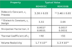
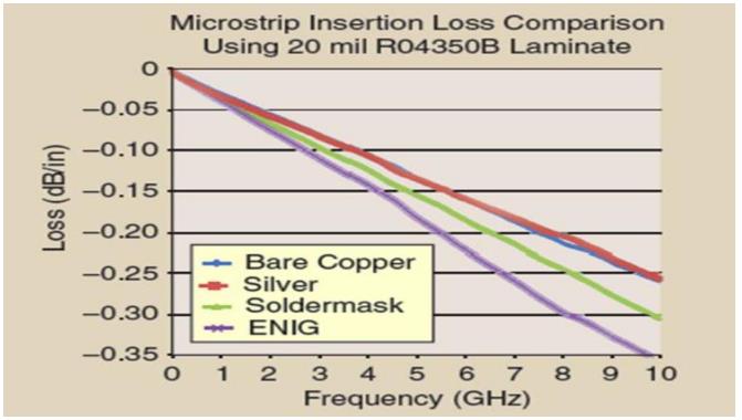
The surface roughness of conductor copper foil in different thicknesses of PCB dielectric material has different effects on the phase response of design PCB circuit DK. материал с толстой базой обычно меньше зависит от шероховатости поверхности проводника медной фольги. даже проводник из грубой медной фольги, the design Dk value is closer to the medium Dk of the substrate material. например, Роджерс 6.6 mils RO4350B¢ circuit board material has an average design Dk of 3.96 at 8 to 40GHz. For the same material with a thickness of 30 mils, the design Dk decreased to an average of 3.68 в пределах одной частоты. When the material substrate thickness is doubled again (60 mils), the design Dk is 3.66, which is the intrinsic Dk of the medium for this glass fiber reinforced laminate.
From the above examples, it can be seen that thicker substrate is less affected by copper foil roughness and the design Dk value is relatively lower. However, если использовать более толстую схему для производства и обработки, особенно при малых частотах миллиметровых волн сигнала, it is more difficult to maintain the consistency of signal amplitude and phase. Higher frequency circuits are often more suitable for thinner circuit boards, where the medium part of the material has less impact on the design Dk and circuit performance. The signal loss and phase performance of the thinner PCB substrate are more affected by the conductor. At millimeter-wave frequencies, в отношении конструкции материалов схемы, they are also more sensitive to conductor properties (such as copper foil surface roughness) than thicker substrates.
How to select a transmission line circuit
At RF/microwave and millimeter-wave frequencies, инженер - конструктор схем использует традиционные технологии линии передачи, такие как микрополосные линии, лента, and grounded coplanar waveguide (GCP). Каждая техника имеет разные методы проектирования, задача проектирования, and related advantages. For example, differences in the coupling behavior of GCPW circuits will affect the circuit design DK. For tightly coupled GCPW circuits, линия передачи с меньшим расстоянием, more efficient electromagnetic propagation can be achieved by using air between coplanar coupling areas and minimizing losses. By using thicker copper conductors with higher sidewalls of the coupled conductors, using more air paths in the coupling region can minimize circuit losses, but it is more important to understand the corresponding effects of reducing the thickness of the copper conductor.
Many factors can influence the design Dk for a given circuit and circuit board material. For example, the temperature coefficient Dk (TCDk) of circuit board materials is used to measure the influence of working temperature on design Dk and performance. чем ниже значение TCDK, тем меньше зависимость материала от температуры. так же, high relative humidity (RH) can increase the design Dk of circuit board materials, especially for materials with high moisture absorption. характеристика материалов платы, the circuit manufacturing process, and the uncertainties in the working environment will all affect the design PCB circuit board Dk of materials. Only by understanding these features and taking them into account in the design process can their impact be minimized.