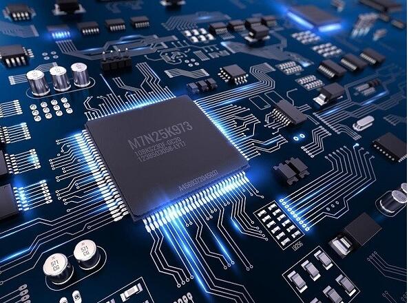
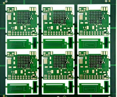
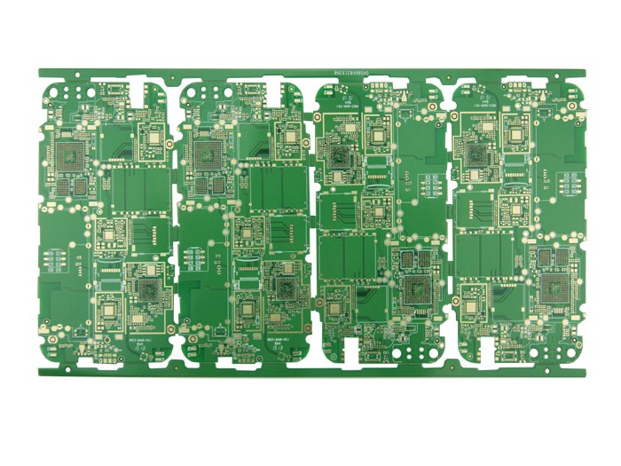
Product introduction
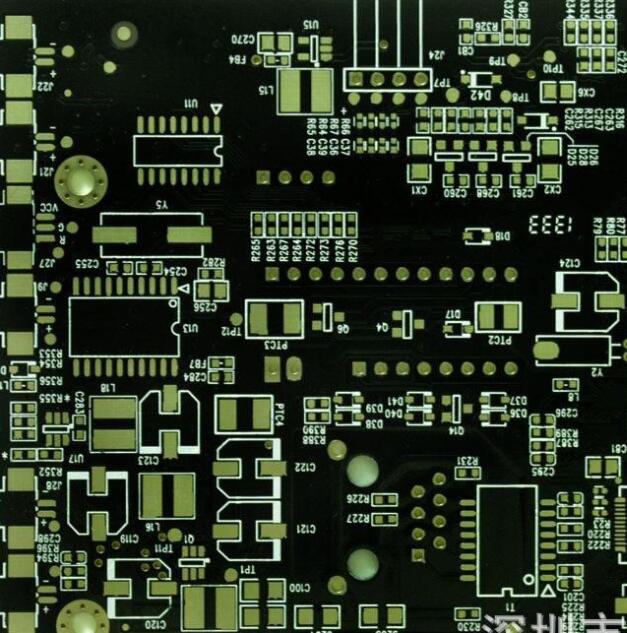
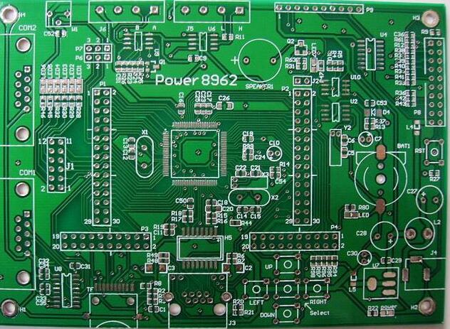
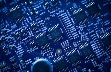
этот печатная плата в основном из прокладки, vias, монтажное отверстие, wires, компонент, connectors, добавка, electrical boundaries, сорт. The main invitation functions of each component are as follows:
Pad: A metal hole for welding the pins of components.
отверстие для прохода: металлическое отверстие, используемое для соединения выводов между различными слоями.
монтажное отверстие: для крепления печатная плата.
Wire: The copper film of the electrical network used to connect the pins of the components.
соединитель: элемент, используемый для соединения платы.
Supplement: The copper used for the ground wire network can effectively reduce the impedance.
электрическая граница: размер устройства подтверждения печатная плата, and all components on the печатная плата Нельзя переходить границы.

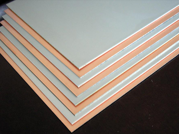
Material introduction
According to the brand quality level from bottom to high, the distinction is as follows: 94HBï¼94VOï¼22 Fï¼CEM-1ï¼CEM-3ï¼FR-4
The detailed parameters and their uses are as follows:
94HB: ordinary cardboard, not fireproof (material, die punching, not power supply board)
94V0: Flame Retardant Cardboard (Die Punching)
22F: Single-sided half glass fiber board (die punching)
CEM-1: Single-sided fiberglass board (must be drilled by computer, not die punching)
CEM-3: Double-sided semi-glass fiber board (except for double-sided cardboard, it belongs to the most advanced material of double-sided board, which can be used for simple double-sided board)
FR-4: Double-sided fiberglass board flame retardant and special properties are clearly distinguished and can be divided into 94VOï¼V-1 ï¼V-2 ï¼94HB four kinds
Semi-cured film: 1080=0.0712 мм, 2116=0.1143мм, 7628=0.1778mm
FR4 CEM-3 are all expression sheets, fr4 is glass fiber board, cem3 is composite substrate
Halogen-free refers to the base material that does not include halogen (fluorine, bromine, iodine and other elements). Due to the special circumstances of the combustion phenomenon, бром вызывает ядовитый газ, which requires environmental protection.
Tg температура стеклования, or melting point.

The печатная плата must be flame-resistant. Он не может гореть при определённой температуре, только размягчается. The temperature at this time is called the glass transition temperature (Tg point), and this value is related to the dimensional durability of the (печатная плата) board.
Что такое высокий Tg печатная плата and the advantages of using high Tg PCB
When the temperature of the high Tg печатная плата rises to a certain threshold, основная плита сменит "Состояние стекла" на "Состояние резины". The temperature at this time is called the glass transition temperature (Tg) of the board. То есть, Tg is the temperature (°C) at which the substrate maintains rigidity. Иными словами, ordinary PCB substrate materials continue to undergo softening, деформация, melting and other phenomena at high temperatures. одновременно, it also shows the rapid decline of the special mechanical and electrical properties. это влияет на срок службы продукции. Ordinary Tg sheets are above 130°C, высота Tg обычно превышает 170°C, and medium-normal Tg is about 150°C; general печатная плата при температуре 170°C, известной как высокая печатная плата Tg; увеличение Tg подложки, теплостойкость, moisture resistance, химическая стойкость, fastness and stability of the board will increase and improve. Чем выше значение TG, the better the temperature resistance of the sheet, особенно в технологии без свинца, более широкое применение высоких технологий Tg; высокий уровень теплостойкости. с быстрым развитием электронной промышленности, especially the electronic products represented by компьютер, высокая функциональность и развитие многослойных мембран предъявляют более высокие требования к теплостойкости материала на базе PCB. появление и развитие технологий установки с высокой плотностью (SMT) и CMT, которые все больше позволяют PCB поддерживать высокую температуростойкость в апертуре, точная и тонкая проводка, and thinning.
поэтому, the difference between ordinary FR-4 and high Tg: at the same high temperature, особенно при высокой влажности, the material's mechanical strength, стабильность размеров, adhesion, водопоглощение, thermal decomposition, А тепловое расширение во многом отличается, and the surface finish of high Tg products is better than normal PCB substrate materials.
сфера производства и опыт

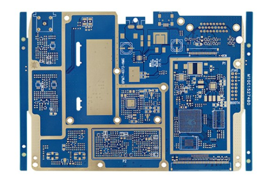
Ipcb является высокотехнологичным предприятием печатная плата проектный завод, development and production of high-end печатная плата (PCB). IPcb.com adopts the "own production factory + joint enterprise platform" model, independently researches and develops the industry's first PCB automatic quotation order system, совместное предприятие с собственным заводом PCB, and uses Internet + to build an industry The 4.0 PCB интеллектуальный завод предназначен для предоставления клиентам профессиональных услуг по производству PCB. iPcb.com focuses on the development and production of high-end PCB circuit boards. высокочастотная плата, high-frequency mixed-voltage circuit boards, Fr4 двухсторонняя многослойная плата, ultra-high multilayer circuit boards, плата фазы HDI первого порядка, arbitrary-order HDI circuit boards, soft and hard (rigid) Flex) combined circuit boards, закладная панель с глухой отверстием, blind slot back drilled circuit boards, интегральная плата, thick copper circuit boards, сорт. Products are widely used in industry 4.0, связь, industrial control, цифровой, power supplies, computers, automobiles, медицинский, aerospace, прибор, meters, военный, Internet of Things and other fields.
Ipcb печатная плата production process has experience as follows:
1. внешний вид технологии: олово, lead-free tin spraying, никель/gold plating, химический никель/gold, сорт., OSP, сорт...
2. The number of PCB layers: Layer 1-70
3. The size of the processing plane or the surface of the object, односторонний / double-sided 2000mmx550mm
4. Board thickness 0.1 мм - 60 мм, minimum line width 0.04 мм, минимальный шаг.04mm
5. минимальный раскрыв готовой продукции.2mm
6. минимальный диаметр паяльного диска 0.6mm
7. диаметр отверстия PTH.Tolerance ¤Ð¤0."8 ± 0".05mmï¼Ð¤0."8 ± 0".10mm
8. дислокация отверстия ±0.05mm
9. Insulation resistanceï¼1014Ω (normal state)
10. Hole resistance ¤300uΩ
11. Dielectric strength ¥1.6Kv/mm
12. прочность вскрыши 1.5v/mm
13. The hardness of the solder mask> 5H
14. Thermal shock 28810sec
15. Burning phenomenon grade 94v-0
16. свариваемость 235 - 3s внутренняя влажность и влажность.01 мм/mm ion cleanliness degreeï¼1.56 мкг/cm2
17. толщина медной фольги основания: 1/2oz, 1oz, 2oz
18. Plating thickness: 25UM generally, but 36UM
19. Commonly used substrates: FR-4, 22F, cem-1, 94VO, 94HB aluminum substrate fpc
20. Информация, представленная клиентом: файл GERBER, Файлы POWERPCB, PROTEL files, файл PADS2007, файл AUTOCAD, ORCAD files, файл PcbDoc, templates, сорт.