Основные шаги проектирование PCB
The basic design process of the circuit board can be divided into the following four steps:

(1) Design of circuit schematic diagram
принципиальная схема схем разработана главным образом с использованием редактора схем Orcad, ALTIUM DESIGNER и т.д.
2) подготовка сетевого доклада
Отчет сети - отчет, демонстрирующий связь между схемой и различными элементами в цепи. It is the bridge and link between the circuit schematic design and the circuit board design (проектирование PCB). Through the network report of the circuit schematic, элементы можно найти очень быстро. The connection between the devices provides convenience for the subsequent проектирование PCB.
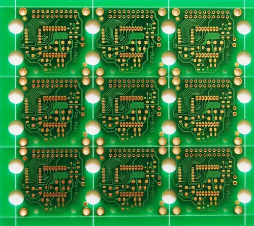
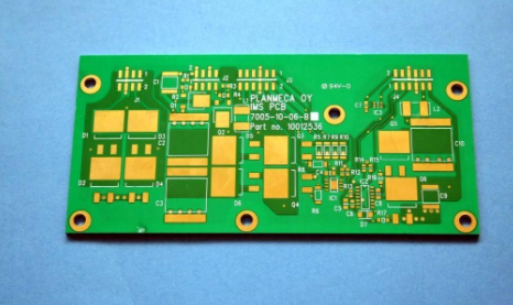
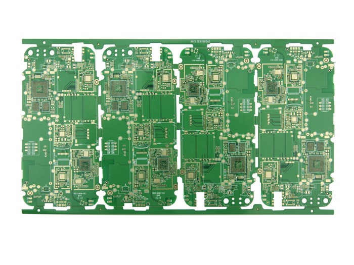
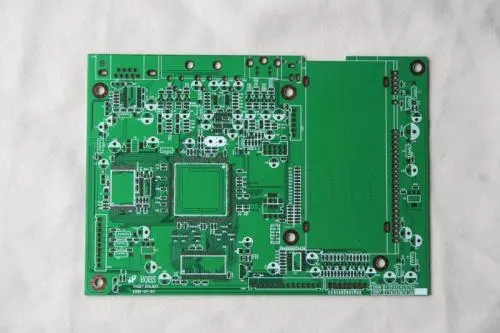
(3) Design of printed circuit board
The design of the printed circuit board is what we usually call the проектирование PCB. It is the final form that the circuit schematic is transformed into. Эта часть сопряжена с более трудным проектированием, чем принципиальная схема схемы. We can use Protel DXP, прокладка, Design tools such as Allegro to complete this part of the design.
(4) Generate printed PCB board reports
After the printed circuit board design is completed, Необходимо создать различные отчёты, such as a pin report, информационный отчёт, a network status report, сорт., and finally a printed circuit diagram is printed.