Content preview:
1 Introduction
2. Signal integrity issues
3. Electromagnetic compatibility issues
4. Power integrity issues
5. General specification for high frequency circuit design
6. General specification for design of digital-analog hybrid circuit

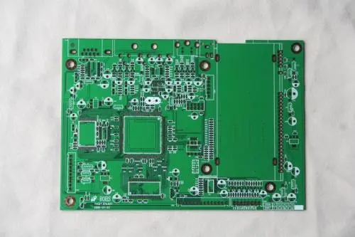
One: The definition of высокочастотная печатная плата
*In digital circuits, зависит ли она от цепи высокой частоты от высоты сигнала вдоль и вниз, not the frequency of the signal.
формула: F2 = 1/(Tr*Ï), тро - повышательная тенденция/fall delay time of the signal.
*F2> 100MHz, it should be considered in accordance with the high-frequency circuit, the following conditions must be designed in accordance with the high-frequency rules
-The system clock frequency exceeds 50MHz
-Using devices with rise/fall times less than 5ns
--Digital/analog hybrid circuit
*Logic device rise/время снижения и ограничение длины монтажа/drop main harmonic spectrum distribution Maximum transmission line maximum transmission
Falling time Tr component F2=1/Fmax=10*distance (microstrip) line distance (microstrip line) ÏTr F2
74HC 13-15ns 24MHz 240 MHz 117cm 91cm
74LS 9.5ns 34 MHz 340MHz 85.5cm 66.5cm
74H 4-6ns 80 MHz 800MHz 35 28
74S 3-4ns 106 MHz 1.1GHz 27 21
74HCT 5-15ns 64 MHz 640MHz 45 34
74ALS 2-10ns 160 MHz 1.6GHz 18 13
74FCT 2-5ns 160 MHz 1.6GHz 18 13
74F 1.5ns 212 MHz 2.1GHz 12.5 10.5
ECL12K 1.5ns 212 MHz 2.1GHz 12.5 10.5
ECL100K 0.75ns 424 MHz 4.2GHz 6 5
Traditional PCB designmethods are inefficient:
Schematic diagram, традиционный метод проектирования и ввода схемы и проводки без каких - либо контрольных точек качества. Every step of PCB design is based on experience. Если проблема найдена, they must start from scratch. трудно найти проблему в тесте функциональности и производительности.
Signal integrity issues:
1. Reflection problem
2. Crosstalk issues
3. Overshoot and oscillation
4. Delay
Reflection problem: echo on the transmission line. Part of the signal power (voltage and current) is transmitted to the line and reaches the load, but there is a part
The points are reflected.
Multipoint reflection
Reason for reflection:
*Impedance mismatch between source and load
*The geometry of the wiring
*The direction of the wiring, via
*Incorrect wire termination
*Transmission through the connector
*Discontinuity of the power plane, сорт.
Crosstalk issues:
*Crosstalk: Coupling between two signal lines
1. Capacitive crosstalk
*This happens when the lines are close to each other at a certain distance.
*Capacitive coupling induces coupling current
2. Inductive crosstalk
*Signal coupling between the primary coil and the secondary coil of the unneeded transformer
*Inductive coupling triggers coupling voltage.
Crosstalk issues:
The parameters of the слой PCB, расстояние между сигнальными линиями, the electrical characteristics of the driving end and the receiving end, а способ соединения концов линии оказывает определенное влияние на последовательное возмущение.
*The crosstalk of capacitance and inductance increases with the increase of load impedance, Поэтому все линии, подверженные воздействию переходного процесса, должны быть соединены с концами линейного сопротивления.
Methods to reduce capacitive crosstalk:
* Separating signal lines can reduce the energy of capacitive coupling between signal lines.
*Using the ground wire to separate the signal line can reduce the coupling of capacitance. To improve effectiveness, заземляющий провод должен заземляться через день/4 inches. (Î wavelength refers to the distance the signal is transmitted per unit time.)
////////////////////////////
General principles:
Punch holes every 2-5cm.
Simulation results of capacitive crosstalk
=============
Ways to reduce perceptual crosstalk
*In order to solve the crosstalk problem of inductance, размер цикла должен быть как можно меньше.
*By avoiding the situation that the signal return line shares a common path, индуктивный переходный процесс, overshoot and oscillation can also be reduced
*Overshoot: Overshoot can cause false clocks or bus data read/Ошибка записи.
*Ringing: The phenomenon of ringing is repeated overshoot and undershoot.
колебание сигнала и окружающие колебания вызваны чересчур большой индуктивностью и ёмкостью на линии. The oscillation belongs to the under-damped state and the surrounding oscillation belongs to the over-damped state.
надлежащий концевой контакт может уменьшить колебания, but it is impossible to completely eliminate it.
Time delay: the different time delays of each signal line in a set of buses
Clock and signal: ensure as wide a window as possible
////////////////////////////
Electromagnetic compatibility issues
*Electromagnetic Interference (EMI) issues
1. проектирование контура, forming antenna effect
2. The slot in the power layer will form a quarter-wavelength antenna
*Dense vias (such as BGA packaged devices)
*Large connectors (especially the backplane)
3. индуктивный элемент.
Примечание: две параллельные индуктивности на поверхности элемента создадут один трансформатор.
Unreasonable return path leads to EMI
EMI caused by incomplete ground plane
Incomplete ground plane can cause large EMI
The simulation without considering the incomplete ground plane is inaccurate
////////////////////////////
Power integrity issues
*High-power high-speed devices: need a large transient current
*The ground layer and power layer are incomplete: 1. деление, via 2. Connector
*Filter capacitor: 3. Quantity, емкость, layout,
Selection of power supply filter capacitor:
The system has both high frequency noise and low C0G (non-ferromagnetic) type frequency noise. It is higher than other types by paralleling large electric 0.01, все в порядке..
Capacitance, Small ESL - устройство, extremely small 0.1. все камеры работают., ESL device can expand the filtering range at high frequency and has better filtering performance
////////////////////////////
Schematic design specification
Signal integrity and electromagnetic compatibility considerations
Correspondence between the schematic diagram and the PCB after the PCB is completed
General rules and requirements
*According to the unified requirements, Выберите размер графика, frame format, графические и буквенные символы в схеме.
* According to the electrical working principle of the product, сборка должна быть расположена вправо - влево, сверху донизу в одну строку или серию.
*When the drawing is arranged, блок питания обычно расположен в левом нижнем углу, the input terminal is on the right, выход слева.
*The working state of the movable components (such as relays) in the picture is in principle in the open and unpowered working position.
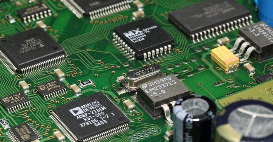
*Use all the power and ground pins of all chips.
////////////////////////////
Signal integrity and electromagnetic compatibility considerations
*Add corresponding filtering/absorption devices to the input and output signals; add silicon transient voltage absorption diode or varistor SVC if necessary
*String resistors on the high-frequency signal output terminal.
*The decoupling capacitors in the high frequency area should be electrolytic capacitors or tantalum capacitors with low ESR
*When determining the value of the decoupling capacitor, для удовлетворения требований, предъявляемых к жилым волнам, выберите менее мощный конденсатор, чтобы увеличить резонансную частоту.
* The power supply of each chip must be added with decoupling capacitors, питание каждого модуля в одном чипе должно быть разделено на конденсатор развязки; если это высокая частота, магнитный шарик/необходимо добавить индуктор.